Leave A Message
Leave A Message
Fill out the form with your requirements and quantities(PCB/ Component Sourcing/ PCBA), and upload your Gerber file & BOM list. We'll provide you with a free quote as soon as possible!
submit
banner
Home

PCB Layout

PCB Layout

What is PCB Layout ?

PCB Layout (Printed Circuit Board Layout), also referred to as PCB Design, is a crucial step in the electronic product development process. It involves the logical arrangement and connection of electronic components based on a predefined circuit diagram to create a fully functional and stable printed circuit board (PCB).

PCB layout goes far beyond simply placing components — it also includes routing, thermal management, electromagnetic compatibility (EMC), and more.


DQS ELECTRONIC has highly skilled teams capable of solving complex design challenges. Our design engineers have over 10 years of experience and are proficient in tools such as PADs PowerPCB, OrCAD, and others.

We have designed a wide range of circuit boards across various industries including consumer electronics, industrial control, medical, military, and telecommunications — from small prototypes to large, complex designs.


Our value-added services (SI, EMC, PI, thermal analysis, DFM analysis, etc.) form the core of our expertise, complemented by EMS manufacturing. This enables us to offer customers a professional one-stop service system — high in quality and competitively priced.


Reliable Design Standards We Offer 

—— IPC Class 2 & 3, JEDEC, and MIL standards available ——

  • #


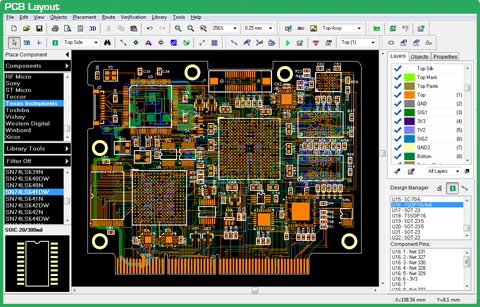
    • Single / Double-Sided / Multilayer: using through-hole, blind/buried via, and laser via technologies

    • Flexible and Rigid-Flex Printed Circuits

    •HDI Designs with Microvias and Advanced Materials – Via-in-Pad, Laser Microvias

    • High-Speed Multilayer Digital PCB Designs – Bus Routing, Differential Pairs, Matched Lengths

    • PCB Design for Space, Military, Medical, and Commercial Applications

  • #


    • Extensive RF and analog design experience (printed antennas, guard rings, RF shielding, etc.)
    • Signal integrity solutions for digital designs (tuned traces, differential pairs, and more)
    • PCB layer stack-up management for signal integrity and impedance control

    • Expertise in DDR, DDR2, DDR3, DDR4, SAS, and differential pair routing

    • High-density SMT designs (BGA, µBGA, PCI, PCIe, cPCI, etc.)

  • #
     

    • Blind and buried vias, flex PCB designs, and all types of rigid-flex boards

    • Low-level analog PCB design

    • Ultra-low EMI designs for MRI applications

    • Complete assembly drawing creation

    • In-Circuit Test (ICT) data generation

    • Design of drill, panel, and cutout drawings

    • Professional fabrication documentation

    • Autorouting for dense PCB layouts


We always strive to provide cost-saving options and deliver value engineering solutions.
Fill out the form with your requirements, and we’ll get back to you shortly.

Custom Order Request

submit
leave a message
If you are interested in our products and want to know more details,please leave a message here,we will reply you as soon as we can.
submit

Our hours

24H

Contact Us: Sales@dqspcba.com

home

products

WhatsApp

Contact