Leave A Message
Fill out the form with your requirements and quantities(PCB/ Component Sourcing/ PCBA), and upload your Gerber file & BOM list. We'll provide you with a free quote as soon as possible!
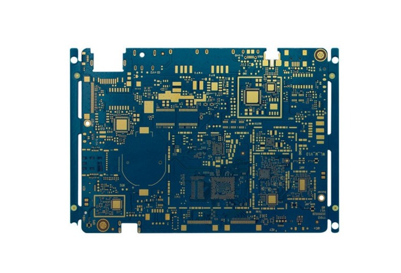
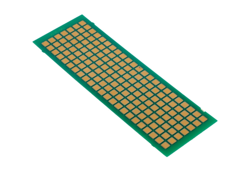
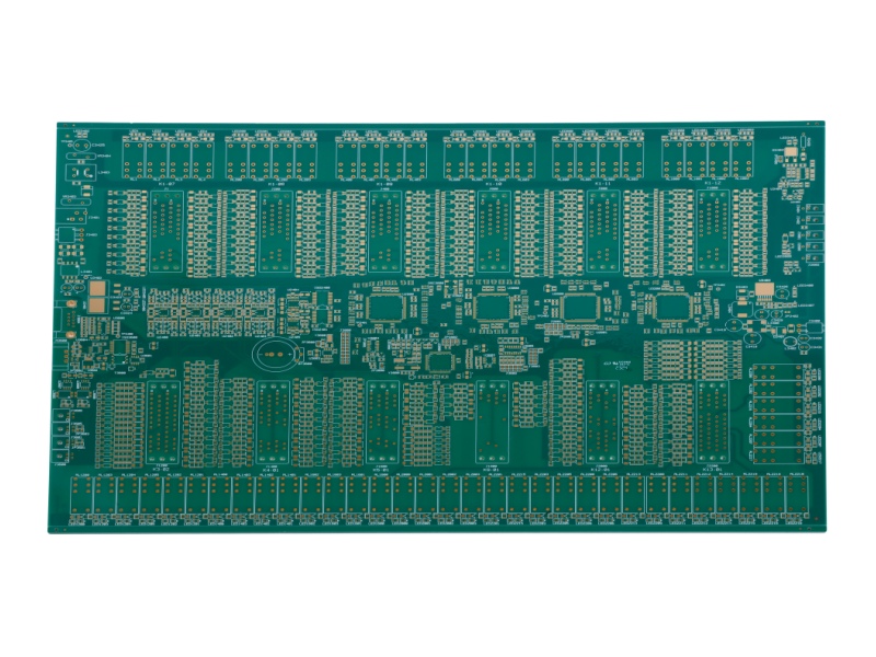
Layer :
8Material :
TG170Board Thickness :
1.2mmMin. Line Width/Space :
0.1/0.1mmSurface Finish :
Immersion GoldApplication :
WIFI ModuleCertificate :
UL&IPC Standard &ISO


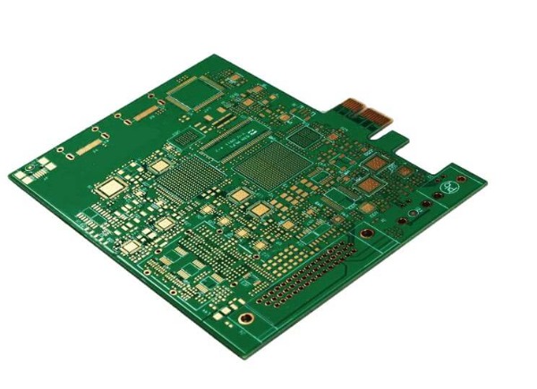
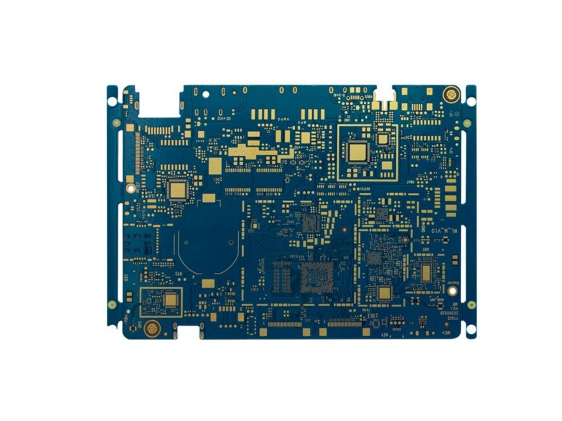
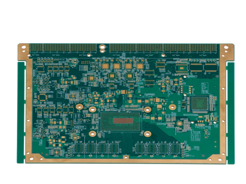
What Is an HDI PCB?
HDI (High-Density Interconnect) printed circuit boards are advanced PCBs with high circuit distribution density. They are manufactured using technologies such as micro-blind vias, laser drilling, electrochemical hole filling, and stacked via structures.
Advantages of HDI PCBs:
High density: Compared with traditional PCB boards, HDI boards have a higher wiring density, which effectively improves the complexity of circuit design and reduces the size of the product.
High reliability: HDI boards have excellent heat resistance, humidity resistance and electrical properties, ensuring the long-term stable operation of electronic equipment.
Excellent electrical and thermal properties: HDI sheet has a low dielectric constant and low coefficient of thermal expansion, which effectively improves the transmission speed of electrical signals and ensures the stable operation of electronic equipment in various environments
Application:
HDI printed circuit boards are widely used in communication equipment, computers, consumer electronics, automotive electronics, and other electronic devices to meet the needs of high-speed data transmission, multi functionalintegration, and small-size design in these fields. It is also widely used in medical equipment, aerospace and defence due to its high wiring density and high reliability.
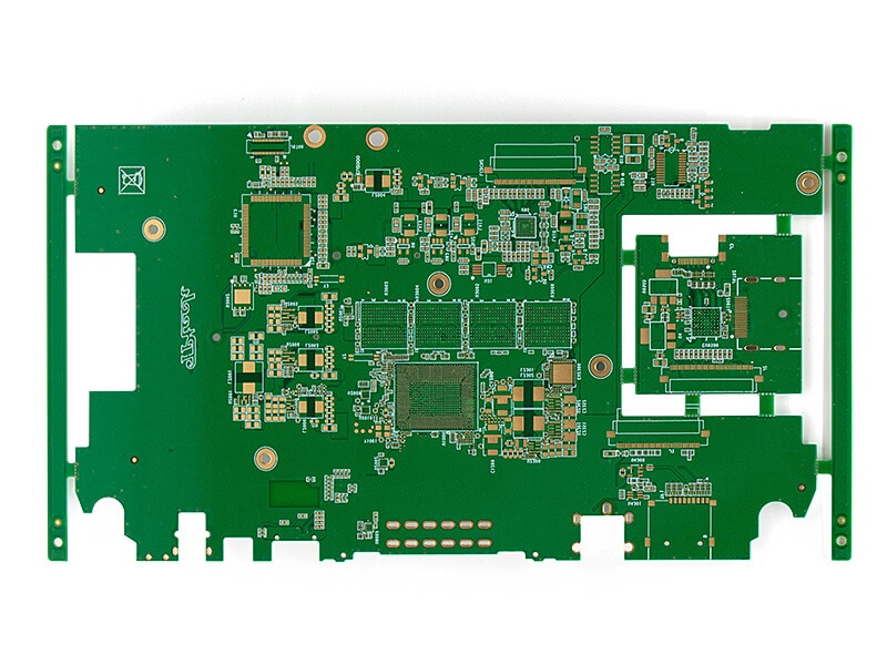
DQS Electronic has introduced high-precision manufacturing equipment, using advanced machinery, excellent metal base materials, and ultra-thick copper processing techniques. We maintain a first-class production line to ensure processing accuracy and quality.
Whether standard or highly complex PCBs – no matter how challenging – simply send us your PCB file, and our engineers will provide a suitable solution.
|
Item |
HDI PCB Capability |
|
Layer |
4-64 L |
| HDI Structure |
1+N+1, 2+N+2, 3+N+3 or any layer interconnection |
|
HDI AVI |
Blind through holes, buried through holes, staggered through holes, stacked through holes, skip through holes |
|
Min. Hole Size |
0.075mm |
|
Min. Line Width/Space |
Rigid PCBs: 2mil/2mil ; Flex PCBs0.025 / 0.025mm |
|
Dielectric Thickness |
Max:0.2mm ; Min:0.06mm |
|
HDI PCB Production Capability |
200000m²/month |
|
Inner copper thickness |
0.5-15oz or more |
|
Outer copper thickness |
0.5-10oz |
|
Surface Finish |
OSP HASL: SMD 40µ to 2000µ’, GND 30µ to 800µ’ ENIG: Au 1µ to 5µ’, Ni 80µ to 200µ’ Immersion Tin: 0.8µm to 1.2µm Immersion Silver: 0.15µm to 0.45µm Hard gold plating: Au 1µ to 50µ’, Ni 80µ to 200µ’ Peelable film: 5mil Carbon Ink: 0.3mil |

We are committed to building a world-leading brand in circuit board assembly services, delivering the most reliable products and support to our customers. Our goal is to set a benchmark in the industry and actively contribute to the advancement of the electronics sector.

Our hours
24H


 IPv6 network supported