Leave A Message
Fill out the form with your requirements and quantities(PCB/ Component Sourcing/ PCBA), and upload your Gerber file & BOM list. We'll provide you with a free quote as soon as possible!
In modern printed circuit board (PCB) design and manufacturing, through holes are indispensable structural units that connect circuit layers, fix electronic components, and assemble finished boards. Among all through-hole types, PTH (Plated Through Hole) and NPTH (Non-Plated Through Hole) are the two most common and foundational categories. Although both start with mechanical drilling, their subsequent manufacturing processes, structural characteristics, electrical properties, and application scenarios are vastly different. Misjudging or misusing PTH and NPTH holes in PCB design will directly lead to circuit short circuits, poor electrical conductivity, unstable assembly, increased production costs, and even product failure. For electronic engineers, PCB designers, and procurement technicians, mastering the core differences between PTH and NPTH is a basic professional skill that determines PCB quality and product reliability. This article will comprehensively analyze PTH and NPTH holes from structural features, manufacturing workflows, electrical and mechanical properties, application scenarios, cost differences, and DFM design specifications, providing a complete reference for industrial application.
1. Basic Definition and Structural Features
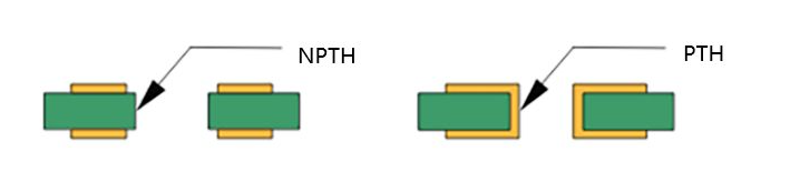
To distinguish PTH and NPTH holes accurately, we first need to clarify their core structural differences, which originate from whether the hole wall is covered with a conductive metal layer after drilling.
PTH refers to electroplated through holes. After mechanical drilling of the PCB substrate, a series of chemical deposition and electroplating processes are adopted to deposit a uniform and dense copper layer on the inner wall of the hole. The thickness of the plated copper layer usually meets the industry standard of 20–25μm, and the hole mouth is covered with solder mask oil or retained copper pad according to design requirements. Structurally, the hole wall of PTH is continuous and conductive, forming a complete electrical channel penetrating all PCB layers. In addition to copper plating, the surface of the hole wall will also undergo tin plating or gold plating in high-precision boards to enhance oxidation resistance and solderability.
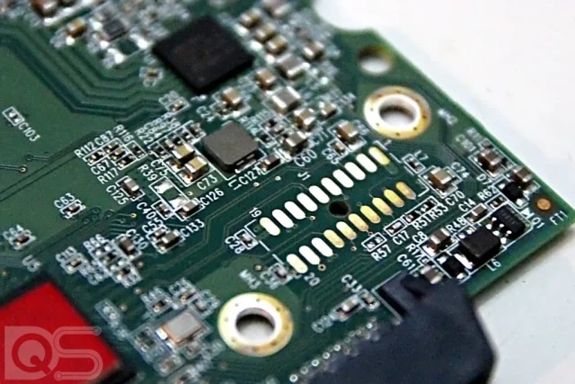
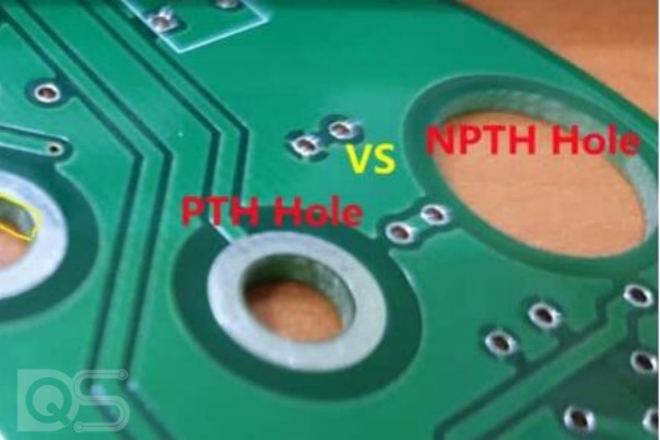
The most intuitive structural feature of PTH holes is the metallic luster on the hole wall. The inner wall is smooth and uniform without substrate exposure. The copper layer runs through the entire hole body, realizing electrical interconnection between the top layer, bottom layer, and inner circuit layers of the PCB. It is the core carrier for multi-layer PCB circuit conduction.
NPTH refers to non-electroplated through holes. After drilling, no chemical copper deposition or electroplating treatment is performed on the hole wall. The inner wall directly retains the original insulating substrate material (glass fiber and epoxy resin), with no conductive metal layer attached. The hole wall is rough, showing the natural texture of the PCB substrate, and has complete insulation performance.
NPTH holes are purely mechanical structural holes with no electrical conduction function. Their core structural attribute is insulation and penetration. They only run through the PCB substrate physically but cannot transmit electrical signals or current. In most cases, NPTH holes do not retain copper pads, and the hole edge is completely separated from the surrounding copper circuits to avoid accidental conduction. Even in a few designs with reserved pads, the hole wall is still insulated, which will not affect circuit performance.
2. Differences in Manufacturing Processes
The structural gap between PTH and NPTH essentially comes from different production processes. PTH requires multiple chemical and electroplating procedures, while NPTH simplifies the process based on drilling, forming obvious differences in production cycle and process difficulty.
The production of PTH holes is a complex multi-step process that combines mechanical processing and chemical electroplating, which is the key process to ensure multi-layer circuit conduction. The complete workflow is as follows: First, perform precise mechanical drilling according to the PCB aperture design standard to form a through hole penetrating the substrate; then conduct hole cleaning and degumming to remove drilling dust, resin burrs, and oil stains on the hole wall, avoiding poor copper adhesion; next, carry out chemical copper deposition, adsorb a thin layer of conductive copper film on the insulating hole wall to form a conductive base; then perform electroplating copper thickening to increase the copper layer thickness to the industry qualified standard; finally, complete surface solder mask treatment, hole shaping and quality inspection.
The whole PTH manufacturing process requires strict control of chemical solution concentration, temperature, current density and processing time. Any process deviation will cause problems such as uneven copper layer, hole wall copper leakage, copper layer falling off, or hole breakage, leading to open circuit failure of the PCB circuit. It is precisely because of the multiple electroplating processes that PTH holes have higher process requirements and longer production cycles.
The production process of NPTH holes is much simpler. The core steps are only mechanical drilling and post-drilling cleaning. After drilling according to the design aperture, only simple dust removal and deburring treatment is needed to remove surface burrs and drilling residues, without any chemical deposition and electroplating processes.
However, it is worth noting that the difficulty of NPTH production lies in anti-plating protection. In the mass production of PCBs, all boards will enter the electroplating production line uniformly. To ensure that NPTH holes are not accidentally plated with copper, manufacturers need to adopt professional hole plugging processes before electroplating, such as colloidal plugging and dry film sealing, to completely isolate the hole wall from the electroplating solution. After the electroplating process is completed, the plugging material is removed to ensure that the NPTH hole wall is completely insulated. This anti-plating process is the key to qualified NPTH holes and also the main technical point that distinguishes them from ordinary drilled holes.
3. Core Performance Differences: Electrical and Mechanical Properties
Electrical conductivity and mechanical stability are the two core performance indicators of through holes, and PTH and NPTH show completely opposite performance characteristics, which directly determine their application functions.
PTH holes have excellent electrical conductivity. The continuous copper layer on the hole wall can realize stable electrical interconnection between all layers of the PCB. It has low resistance, strong current carrying capacity, and stable signal transmission performance. It can adapt to high-frequency signal transmission and high-current circuit working scenarios, and will not produce signal attenuation or open circuit problems under normal working conditions. All through-hole component welding, circuit layer conduction, and via signal transmission in PCBs rely on PTH holes.
NPTH holes have absolute insulation. There is no conductive medium on the hole wall, so they cannot conduct current and signals at all. They are completely electrically isolated from the PCB internal circuits and external components. This insulation performance avoids the risk of circuit short circuit and signal crosstalk, which is very suitable for structural assembly scenarios that need to avoid electrical contact.
In terms of mechanical strength, PTH holes have better structural stability. The electroplated copper layer is tightly attached to the substrate hole wall, which effectively enhances the hardness and toughness of the hole body, prevents hole wall cracking and substrate delamination, and can withstand repeated welding and mechanical vibration. The copper pad at the hole mouth also increases the welding contact area, improving the firmness of component assembly.
The mechanical strength of NPTH holes depends entirely on the PCB substrate material. The hole wall is relatively rough and has no metal layer protection. Long-term vibration and extrusion are easy to cause substrate wear and burr falling off. However, NPTH holes have better stress relief performance. As pure insulating holes, they will not produce metal fatigue and oxidation corrosion failure, and have longer service life in fixed assembly scenarios.
4. Typical Application Scenarios of PTH and NPTH Holes
The functional differences between PTH and NPTH determine their exclusive application scenarios. Standardized hole selection is the basis for reasonable PCB design and stable product operation.
PTH holes focus on electrical conduction and component welding, and are widely used in all circuit connection scenarios. First, they are used for through-hole component welding, including resistors, capacitors, inductors, connectors, pin headers and other plug-in components. The pins pass through PTH holes and are welded with the hole wall copper layer to realize component fixation and circuit conduction. Second, they are used for multi-layer PCB interlayer vias, realizing electrical connection between top layer, bottom layer and inner buried circuits, which is the core of multi-layer PCB circuit design. In addition, PTH holes can also be used for high-current conductive holes and grounding holes to ensure stable circuit grounding and safe current transmission.
NPTH holes focus on mechanical positioning, fixing and insulation assembly, and never participate in any electrical conduction. The most common applications are PCB mounting holes and screw fixing holes, which are used to fix the circuit board on the shell, bracket and equipment base to prevent displacement and vibration. Second, they are used for positioning holes and tooling holes in PCB production and assembly, assisting automated equipment in precise board positioning and processing. In addition, NPTH holes are also used for assembly avoidance holes and insulating limit holes, avoiding contact between metal structural parts and PCB circuits to prevent short circuit faults. In connector assembly and module positioning scenarios, NPTH holes are also essential auxiliary structural holes.
5. Cost, Yield and DFM Design Guidelines
In industrial mass production, hole selection also needs to comprehensively consider production cost, yield and design manufacturability (DFM).
In terms of cost, PTH holes are more expensive. Multiple processes such as chemical copper deposition and electroplating increase material consumption, labor time and equipment loss, resulting in higher unit production costs and longer delivery cycles. NPTH holes have simple processes, fewer production steps, lower failure rates, and more cost advantages, which are suitable for large-scale structural hole production.
In terms of yield control, PTH holes are prone to defective problems such as uneven copper plating, hole wall voids, copper layer peeling and plug holes, with relatively strict quality inspection standards. NPTH holes have low process difficulty, few defective products, and high production yield, but the key control point is to prevent accidental copper plating on the hole wall. Once the anti-plating protection fails, the NPTH holes will be mistakenly plated into PTH holes, resulting in board scrapping.
In terms of DFM design specifications, designers need to strictly distinguish hole functions: all holes involving circuit conduction and component welding must use PTH; all purely mechanical fixing and positioning holes must use NPTH to save costs and avoid electrical risks. In addition, the aperture tolerance of PTH holes is stricter to ensure welding accuracy, while NPTH holes can appropriately relax the tolerance range on the premise of meeting assembly requirements.
6. Summary
In short, the essential difference between PTH holes and NPTH holes lies in conductive plating or not, which derives the differences in process, performance and application. PTH holes are conductive functional holes, with complex processes, stable electrical performance and wide circuit conduction applications, which are the core of PCB electrical connection; NPTH holes are insulating structural holes, with simple processes, low cost and reliable mechanical performance, which are the guarantee of PCB assembly stability.
For PCB designers and manufacturers, standardized selection of PTH and NPTH holes according to functional requirements can not only optimize product performance and improve circuit stability, but also effectively control production costs, reduce defective rates, and improve the overall quality and market competitiveness of electronic products. In the increasingly sophisticated electronic manufacturing industry, mastering these basic process differences is the first step to achieve high-quality PCB design and production.

We are committed to building a world-leading brand in circuit board assembly services, delivering the most reliable products and support to our customers. Our goal is to set a benchmark in the industry and actively contribute to the advancement of the electronics sector.



Our hours
24H


 IPv6 network supported