Leave A Message
Fill out the form with your requirements and quantities(PCB/ Component Sourcing/ PCBA), and upload your Gerber file & BOM list. We'll provide you with a free quote as soon as possible!
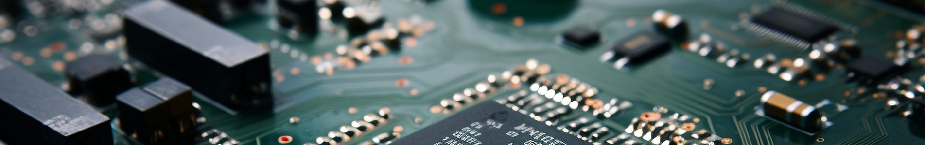
In the rapidly evolving world of electronics, devices are becoming increasingly compact, powerful, and efficient. Have you ever wondered how smartphones, smartwatches, and high-performance computing devices pack so much power into such minuscule frames? The answer lies in a revolutionary technology known as SMD (Surface-Mount Device).
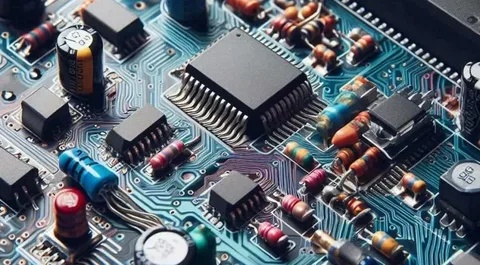
SMDs are the building blocks of modern electronic circuits, designed to be mounted directly onto the surface of a Printed Circuit Board (PCB). Unlike their predecessor—the Through-Hole Technology (THT) components, which required wires to pass through drilled holes in the board—SMDs are soldered flat onto the PCB's surface using Surface-Mount Technology (SMT). This fundamental shift in manufacturing has enabled the production of smaller, lighter, and more sophisticated electronic devices.
This comprehensive guide will walk you through everything you need to know about SMD components, exploring their classifications, distinct advantages, and the cutting-edge trends shaping their future.
1. The Classification of SMD Components
The world of SMDs is vast and diverse. To navigate it effectively, engineers and designers classify these components based on their functional roles and physical package types.
A. Classification by Function
From a functional perspective, SMDs can be broadly categorized into three main groups:
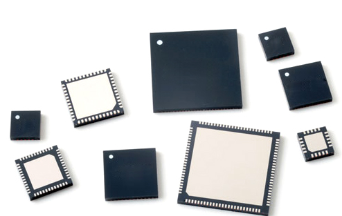
B. Classification by Package Type
The physical housing of an SMD, known as its "package," is crucial for thermal management, electrical performance, and automated assembly. As technology advances, packages have evolved to become smaller and more efficient:
2. The Distinct Advantages of SMD Technology
Why has the electronics industry almost entirely shifted from through-hole to surface-mount technology? The reasons are compelling:
3. Emerging Trends and the Future of SMD Technology
As the demand for smarter, faster, and more energy-efficient electronics grows, SMD technology continues to push the boundaries of physics and engineering. Here are the key trends defining the future of SMDs:
A. The Relentless Drive Toward Miniaturization
The mantra of the electronics industry is "smaller, faster, cheaper." We are witnessing the mainstream adoption of ultra-miniature packages like 01005 (0.4 mm × 0.2 mm) and even smaller 008004 components. These microscopic parts challenge traditional pick-and-place accuracy and soldering techniques, pushing manufacturers to develop more precise optical inspection systems and advanced soldering pastes.
B. High-Frequency and Low-Loss Materials for 5G and IoT
The rollout of 5G networks and the explosion of the Internet of Things (IoT) require components that can handle extremely high frequencies (millimeter-wave spectrum) with minimal signal loss. In response, the industry is shifting toward advanced low-loss dielectric materials and novel nanocomposite substrates. These materials ensure signal integrity and reduce electromagnetic interference (EMI) in crowded circuit environments.
C. Advanced Thermal Management Solutions
As chips become more powerful while shrinking in size, heat density becomes a critical bottleneck. Future SMD packages, particularly for power electronics and high-performance processors, are incorporating advanced thermal interface materials (TIMs) and innovative internal structures like embedded heat spreaders or diamond-based substrates to efficiently channel heat away from the core.
D. System-in-Package (SiP) and Heterogeneous Integration
We are moving away from the traditional separation of components. System-in-Package (SiP) technology integrates multiple active dies (like an MCU, memory, and sensors) and passive components into a single, compact module. This heterogeneous integration offers the functionality of a complex circuit board within the footprint of a single SMD, drastically simplifying the PCB design process for OEMs.
E. Intelligent and Eco-Friendly Manufacturing
The factories of the future are smart. The production of SMD-based PCBs is increasingly relying on AI-driven optical inspection (AOI) and automated X-ray inspection (AXI) to detect microscopic defects in real-time. Furthermore, driven by stringent global environmental regulations, the industry is aggressively transitioning toward fully lead-free, halogen-free, and recyclable SMD components.
Conclusion
Surface-Mount Devices (SMDs) are undeniably the silent heroes powering the modern technological renaissance. From the smartphone in your pocket to the sophisticated servers running artificial intelligence algorithms, SMDs make it all possible through their unparalleled combination of miniaturization, performance, and reliability.
Understanding the classifications and advantages of SMDs is crucial for any engineer, designer, or tech enthusiast. As we look toward a future filled with 6G communications, ubiquitous AI, and flexible electronics, SMD technology will continue to evolve, breaking today's limitations and enabling the next generation of groundbreaking innovations. Embracing these advancements is not just an option for electronics manufacturers—it is an absolute necessity to thrive in the competitive landscape of tomorrow.

We are committed to building a world-leading brand in circuit board assembly services, delivering the most reliable products and support to our customers. Our goal is to set a benchmark in the industry and actively contribute to the advancement of the electronics sector.


Our hours
24H

 IPv6 network supported