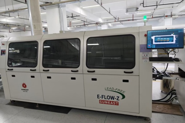
Wave Soldering is an automated mass welding process specially designed for PCB through-hole assembly, which was invented in the 1950s and has been continuously optimized and upgraded to adapt to modern high-efficiency and high-quality production standards. Different from manual welding and reflow soldering, the core feature of Wave Soldering is to use mechanical equipment to melt solder alloy into liquid state and form a continuous, stable flowing solder wave. During production, the PCB board with inserted through-hole electronic components is transported by the conveyor track at a fixed speed and angle, so that the welding surface of the board fully contacts the solder wave, completing the synchronous welding of component pins and PCB pads in one go.
The complete Wave Soldering process is standardized and streamlined, mainly including four core links: flux spraying, preheating, wave welding, and cooling. Firstly, uniform flux is sprayed on the PCB welding surface to remove oxide layers on pads and component pins, enhance solder wettability, and effectively avoid virtual welding and missing welding defects. Secondly, the preheating stage slowly raises the PCB temperature to volatilize flux volatile components and prevent high-temperature impact from causing PCB deformation and component damage. Then comes the core welding link, where the PCB passes through the dual solder wave system. The first turbulent chip wave fully penetrates dense component pins to eliminate hidden welding dead zones, while the second smooth laminar wave trims solder joints to remove excess solder and avoid tin bridging and burrs. Finally, natural or forced cooling is carried out to rapidly solidify the solder, forming firm and conductive solder joints.
It is worth noting that modern Wave Soldering technology has achieved green and low-carbon upgrading. Traditional leaded solder has been gradually replaced by lead-free tin alloy solder, which meets international environmental protection standards while maintaining excellent welding performance, making it applicable to high-standard electronic product production worldwide.
In the PCB assembly production system, Wave Soldering undertakes multiple core functions such as electrical connection, mechanical fixation, and production efficiency improvement, solving the pain points of low efficiency and unstable quality of traditional manual welding.
First of all, the most fundamental function is to realize reliable electrical conduction. The core value of PCB assembly is to build a complete circuit conduction system. Wave Soldering enables the molten solder to fully wrap the component pins and penetrate the PCB through-holes. After cooling and solidification, it forms dense, crack-free solder joints, ensuring stable current transmission between components and circuit boards. This effectively avoids circuit failure problems such as open circuit and poor contact caused by insufficient welding, and lays a foundation for the stable operation of electronic products.
Secondly, it provides strong mechanical fixation for electronic components. Most through-hole components such as large electrolytic capacitors, connectors, and power inductors are large in size and heavy in weight. Ordinary welding processes cannot provide sufficient fixing force, and components are prone to loose pins and falling off under external vibration, temperature change and other environments. The solder joints formed by Wave Soldering have high structural firmness, which can firmly lock components on the PCB board, improve the shock resistance and stability of the whole machine, and adapt to complex application scenarios such as industrial equipment and automotive electronics.
In addition, Wave Soldering greatly improves the efficiency of mass production. Manual welding can only operate on a single solder joint, which is time-consuming and labor-intensive, and cannot meet the demand for large-scale batch production. Wave Soldering realizes full-board synchronous welding. A complete PCB board can finish all through-hole component welding in a few seconds, and the production efficiency is dozens of times that of manual welding. It can stably support the daily output of tens of thousands of PCBs for manufacturing enterprises, greatly shorten the production cycle and reduce labor costs.
The Irreplaceable Importance of Wave Soldering for Electronic Manufacturing
With the rapid development of miniaturized and high-density electronic products, SMT surface mount technology has become the mainstream of precision component welding, but Wave Soldering still has irreplaceable strategic importance in the PCB assembly industry, and has become a key process to balance product quality and production cost.
In terms of product applicability, Wave Soldering is the optimal solution for through-hole component welding. At present, most electronic products adopt a hybrid assembly mode of SMT patch + through-hole plug-in. High-power, large-size, and high-stability required components still rely on through-hole assembly technology. Wave Soldering has unique advantages in welding such components, with strong compatibility and no need for complex auxiliary fixtures, which can perfectly adapt to the production needs of various industrial electronic devices, household appliances, and power equipment.
In terms of quality control, standardized Wave Soldering process effectively reduces product defect rates. The automated mechanical operation avoids human errors such as uneven solder amount, offset welding and missing welding in manual operation. Through precise control of temperature, wave height, and transmission speed, the consistency of each solder joint is guaranteed. Stable welding quality greatly reduces the rate of defective products, lowers the after-sales maintenance cost of enterprises, and improves product market competitiveness.
In terms of enterprise production benefits, Wave Soldering balances high efficiency and low cost. Compared with high-precision reflow soldering equipment, Wave Soldering equipment has lower operation and maintenance costs, higher production throughput, and is more suitable for medium and large batch production. For electronic manufacturing enterprises, the popularization and application of Wave Soldering not only improves the automation level of the production line, but also optimizes the production cost structure, helping enterprises gain advantages in the fierce market competition.
Moreover, with the continuous upgrading of industrial manufacturing standards, modern Wave Soldering technology has been combined with intelligent monitoring systems. It can realize real-time detection of solder joint quality, automatic early warning of process abnormalities, and traceability of production data, which further promotes the intelligent and standardized development of PCB assembly production and meets the high-quality production requirements of high-end electronic products.
Conclusion
From traditional manual welding to modern automated wave soldering, the iteration of Wave Soldering technology has always accompanied the development of the electronic manufacturing industry. It is not only a key process to realize the welding of PCB through-hole components, but also an important guarantee for the stability, durability and mass production of electronic products. Although the electronic assembly technology is constantly innovating, Wave Soldering, with its unique applicability, high efficiency and stability, will always be an indispensable core link in PCB assembly production. For electronic manufacturing enterprises, mastering and optimizing the Wave Soldering process is not only the basis for ensuring product quality, but also a key factor in improving production efficiency and enhancing core market competitiveness.






 IPv6 network supported