Leave A Message
Fill out the form with your requirements and quantities(PCB/ Component Sourcing/ PCBA), and upload your Gerber file & BOM list. We'll provide you with a free quote as soon as possible!
1. What Is PCB X-ray Test?
PCB X-ray test is a non-destructive inspection (NDI) technique that uses penetrating X-ray radiation to image the internal structure of a printed circuit board or an assembled PCBA. Unlike AOI (Automated Optical Inspection), which can only see the outer surfaces, X-ray reveals what lies beneath: solder joints hidden under components, the inner layers of multilayer boards, package structures, and even the internal material state of a single solder ball.
Because it is non-destructive, X-ray inspection does not damage or alter the board in any way. Every unit can be checked quickly, defects can be caught before they reach the customer, and boards that pass can continue into the next stage of production without risk.
2. Why X-ray? The Limits of the Human Eye
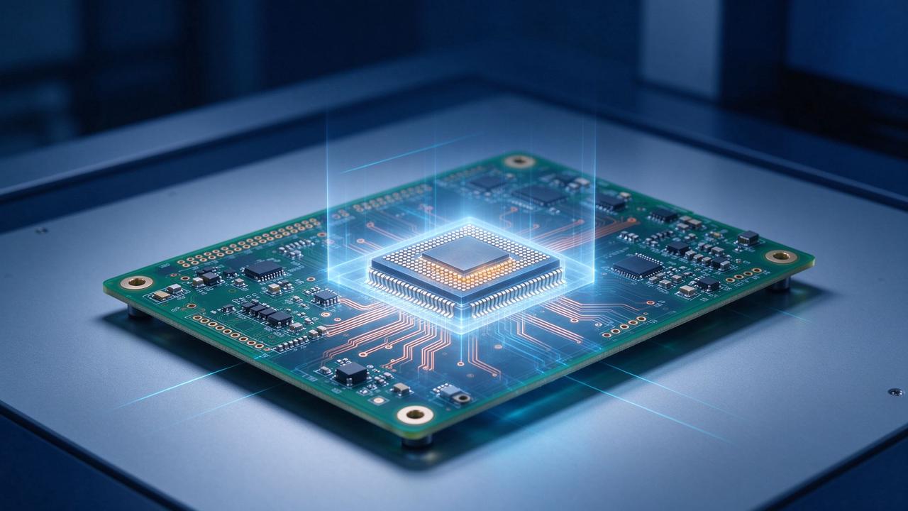
The modern PCB is no longer a flat, inspectable object. Consider a single BGA (Ball Grid Array) chip: hundreds of tiny solder balls sit under a large package, completely hidden from view. If one of those balls has a void, an open connection, or a solder bridge to its neighbor, no camera or operator will ever spot it from above. The board may pass every optical check and still fail catastrophically in the field.
X-ray inspection answers exactly these questions. It verifies that hidden solder joints are properly wetted and connected, that no bridges exist between adjacent balls, that vias and through-hole joints are filled, and that component placement and alignment are correct—even in stacked or shielded assemblies.
3. 2D vs 3D: Why Depth Changes Everything
Traditional 2D X-ray gives you a flat, top-down projection. It is fast, and it is good at spotting bridges and gross defects. But it has a fundamental weakness: everything is superimposed into a single image. In a densely populated board, the solder joints you care about are often hidden behind other components, and a 2D image simply cannot tell you the height or exact depth of a feature.
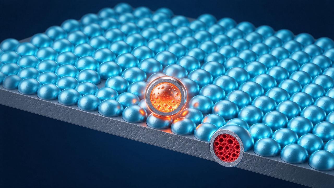
3D X-ray inspection—sometimes called CT (computed tomography)—rotates the X-ray source and detector around the board and reconstructs a true three-dimensional volume. Instead of one flat shadow, you get a sliceable, rotatable 3D model of the assembly. Now you can inspect one single solder ball in isolation, measure a void accurately, and find defects that would be completely invisible in a 2D projection.
4. Meet the 3D SCIENSCOPE X-Ray System
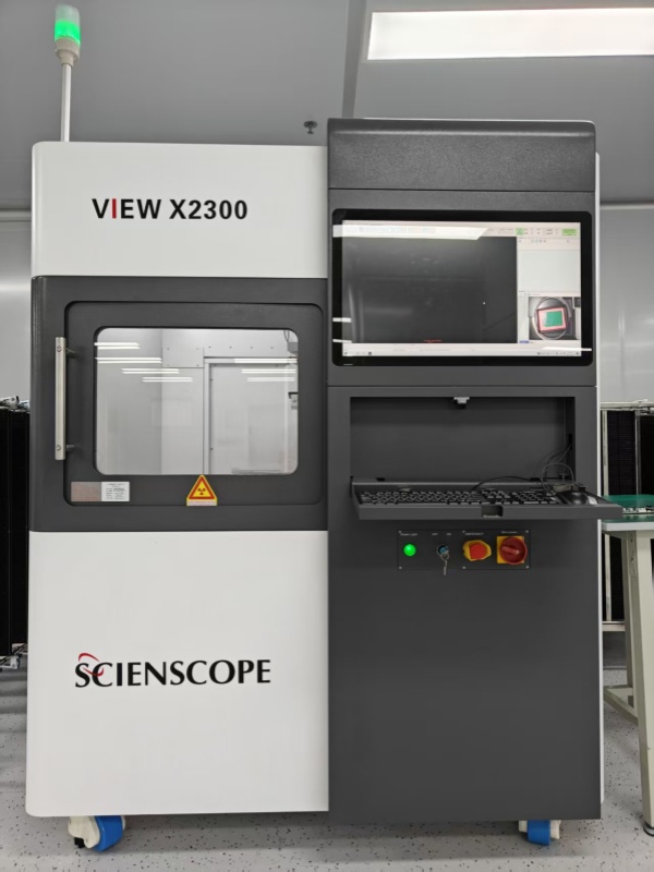
This is where the 3D SCIENSCOPE X-Ray machine comes in. Built for the realities of high-density, high-reliability electronics manufacturing, our system combines fast 2D inspection with true 3D CT capability in a single platform—so you no longer have to choose between speed and depth.
Here is what sets the 3D SCIENSCOPE apart:
True 3D computed tomography. Rotate, slice, and measure any solder joint or feature in three dimensions. Inspect a single BGA ball in isolation, free from the clutter of surrounding components.
Precise void analysis. Quantify void percentage, location, and cumulative volume inside solder joints against IPC standards—the kind of data optical inspection can never provide.
Automated, repeatable inspection. From rapid 2D screening to targeted 3D analysis, the workflow is designed to keep pace with production lines while delivering trustworthy, repeatable results.
Intuitive operation. Powerful imaging does not have to mean complicated software. Our system is engineered so engineers can get the answers they need quickly and confidently.
5. What Can PCB X-ray Inspection Catch?
Put simply: the defects that matter most in modern electronics.
BGA and CSP solder joints. Voids, opens, bridges, and head-in-pillow defects hidden beneath the package.
QFN, LGA and other leadless packages. Solder coverage and voiding under thermal pads that directly affect reliability.
Through-hole and press-fit joints. Fill quality and barrel integrity that optical systems cannot verify.
Inner-layer and plated-through connections. Defects deep inside multilayer boards and vias.
Component placement and shielding. Misalignment, missing components, and internal structures.
6. A Smarter Way to Look Inside Your Boards
In an industry where a single hidden defect can cause expensive recalls and field failures, inspection depth is not a luxury—it is a necessity. PCB X-ray testing turns the "unknown" inside your boards into measurable, verifiable data.
With the 3D SCIENSCOPE X-Ray system, you get the full picture: the speed to keep up with production, and the 3D depth to truly understand every critical joint. If you manufacture, assemble, or qualify high-reliability electronics, it is time to look beyond the surface.
Want to see what is really inside your boards? Contact us today for a demonstration of the 3D SCIENSCOPE X-Ray system.

We are committed to building a world-leading brand in circuit board assembly services, delivering the most reliable products and support to our customers. Our goal is to set a benchmark in the industry and actively contribute to the advancement of the electronics sector.



Our hours
24H


 IPv6 network supported