Leave A Message
Fill out the form with your requirements and quantities(PCB/ Component Sourcing/ PCBA), and upload your Gerber file & BOM list. We'll provide you with a free quote as soon as possible!
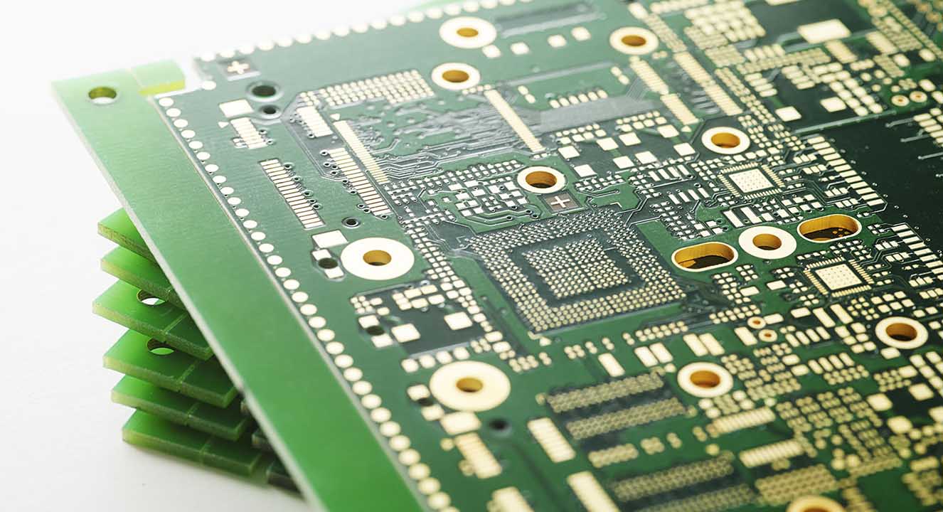
In today's ubiquitous smart devices, a small circuit board (PCB) behind, carrying the wisdom of countless engineers and the crystallisation of precision technology. As the core carrier of electronic equipment, PCB (Printed Circuit Board) manufacturing process integrates material science, precision processing and automation technology. This article to the industry standard process as the main line, analysis of the seven core stages of PCB manufacturing, to bring you an in-depth understanding of the art of precision manufacturing of this modern industry.
1. Schematic Design
Use Altium Designer, Cadence and other software to draw circuit logic, through the DRC (Design Rule Check) to ensure that the component layout and wiring in line with the electrical rules, while the need to take into account the signal integrity, electromagnetic compatibility (EMC) and other factors, to optimise the alignment of the width and spacing, such as high-speed signal lines need to be reserved for the principle of 3W (line width = 3 times the line spacing).
2. File output Conversion
Generating (with graphic data for each layer), drilling files (Excellon format) and BOM lists as production instructions, the engineer converts the Gerber files to film, marking the conductive areas by means of black ink and the transparent areas marking the non-conductive substrate.
1. Substrate Selection
FR-4 epoxy glass cloth substrate (dielectric constant 4.5-5.5) is commonly used, while Rogers or polytetrafluoroethylene (PTFE) materials are used for high-frequency boards.
2. Cut Lamina TIon
Cut the large boards into working boards according to the order size, with the error controlled within ±0.1mm to ensure the subsequent lamination alignment.
3. Surface Cleaning
Removal of copper surface oxides with plasma cleaner to improve subsequent plating adhesion。
1. Coated Photoresist
Liquid photographic ink is uniformly sprayed on the copper surface and pre-baked in a vacuum environment to form a solid film layer.
2. Exposure and Developing
The film pattern is transferred to the Photoresist by UV light, and the developer (sodium carbonate solution) dissolves the unexposed area, preserving the circuit pattern.
3. Graphic Plating
A 20-30μm thick copper layer is plated over the graphic area to enhance conductivity; selective tin plating protects the line edges.
1. Acid Etching
Vertical etching was performed using FeCl₃ or H₂SO₄+H₂O₂ solutions at a rate of 0.5-2oz/min, with line width tolerances controlled to ±0.02mm.
2. Film Stripping
Sodium hydroxide solution removes residual Photoresist to expose the copper surface in the non-line area.
3. AOI Inspection
Automatic detection of line widths, notches and other defects with a 200x magnifying glass.
1. Lamination Process
The multilayer board adopts high temperature and high pressure technology to closely combine the inner layer with the insulating layer, and the prepreg (PP sheet) fills the gap between the layers to achieve interlayer conduction.
2. Laser Drilling
Precise machining of microvias is achieved for high-density interconnect (HDI) boards using C using a drill with a diameter of only 100 microns.
3. Mechanical drilling
The high-speed rotating drill bit is in direct contact with the PCB board and removes the material by mechanical cutting to form the desired hole.
1. Chemical Copper Deposition: A thin layer of chemical copper is chemically deposited on the substrate of the drilled, non-conductive hole walls to serve as a substrate for subsequent copper plating. This process is essential for achieving electrical connections between PCB layers and is one of the key steps in ensuring the overall performance of the board. This step requires circulation and filtration of the solution to prevent contamination by impurities.
2. Surface Treatment Process Selection
• HASL:Hot air solder leveling (thickness 2-5μm), low cost but easy to oxidise
• ENIG:High temperature resistant electroless nickel gold (Ni 3-5μm/Au 0.05-0.1μm), suitable for high density pads
• Sinking silver: excellent electrical conductivity, but only 6 months storage period
3. Solder Resist Printing
Screen printing or LDI exposure is used to cover the non-soldered areas with a soldermask thickness of 10-30 μm.
• Visual inspection: inspectors with the help of natural light or specific lighting equipment, in the magnifying glass (generally 5 - 10 times) with the aid of a comprehensive view of the PCB board. Mainly check whether the line has a short circuit, circuit breakers, whether the copper foil is scratched, exposed copper phenomenon, whether the pad is complete.
• Automated Optical Inspection (AOI)
AOI equipment uses high-speed and high-precision optical imaging system and image processing algorithms to perform rapid laser scanning of PCB boards to compare design drawings. It can detect whether the line width and spacing of the line are in accordance with the design standard, and whether the size and position of the pads are accurate.
2. Electrical Performance Testing
• Flying Probe Test: Through the movable probe contact with the test point on the PCB board, measuring the line on/off, resistance, capacitance and other parameters, to verify the connectivity.
• In-Circuit Testing (ICT): Comprehensive testing of components and circuits on circuit boards is carried out by fixing test probes to specific test points on the PCB board via a pin-bed fixture.
3. Impedance Testing
TDR equipment inspects high-speed signal boards (±10% tolerance) by sending a pulse signal to the transmission line on the PCB and then analysing the reflected signal to determine the impedance characteristics of the transmission line.
4. X-Ray Inspection
Used to detect defects inside the PCB board, such as the filling of blind holes, buried holes, and whether there are any breaks, short circuits and other problems in the internal lines, and to observe the internal quality of BGA pads .
From the design file to the finished product shipment, a PCB needs to go through 200+ processes, and the precision error of each process needs to be controlled at the micron level. With the continuous development of science and technology, PCB manufacturing is moving towards higher density, smaller aperture, and more environmentally friendly direction. Understanding and mastering these core technologies to keep up with the times is a must for every PCB manufacturer. If you have any manufacturing pcb needs, please feel free to contact us, we will provide one-stop service for you.
Email: sales@dqspcba.com

We are committed to building a world-leading brand in circuit board assembly services, delivering the most reliable products and support to our customers. Our goal is to set a benchmark in the industry and actively contribute to the advancement of the electronics sector.


Our hours
24H

 IPv6 network supported