Leave A Message
Fill out the form with your requirements and quantities(PCB/ Component Sourcing/ PCBA), and upload your Gerber file & BOM list. We'll provide you with a free quote as soon as possible!
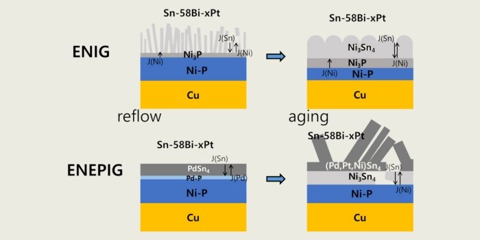
ENEPIG (Electroless Nickel Electroless Palladium Immersion Gold) is an important technological breakthrough in the field of PCB surface treatment in recent years. This process provides an ideal surface protection solution for modern high-density interconnected PCBs by depositing nickel, palladium and gold layers on copper pads in sequence.
1. Micro-etching of copper surface: removing the oxide layer to ensure a clean surface
2. Activation treatment: prepare for subsequent chemical plating
1. Thickness: usually 3-6 μm
2. Function: Acts as a diffusion barrier between copper and precious metals
3. Features: Phosphorus content is controlled at 7-9% to obtain optimal performance
1. Thickness: 0.05-0.15 μm
2. Function: Prevent nickel layer from oxidation and improve reliability
3. Features: More corrosion-resistant than gold layer, lower cost
1. Thickness: 0.03-0.05 μm
2. Function: Provide excellent solderability and bonding performance
3. Features: Extremely thin but effective
Excellent welding performance |
Wide package compatibility |
Long-term reliability guarantee |
Cost-Benefit Analysis |
|
1. Gold layer ensures good solder wetting 2. The palladium layer prevents poor soldering due to nickel oxidation 3. Suitable for lead-free soldering process |
1. Support advanced packaging such as SMT, BGA, CSP, etc. 2. Suitable for fine pitch components below 0.3mm 3. Compatible with gold wire and copper wire bonding processes |
1. The nickel layer effectively blocks copper diffusion 2. Triple protective layer to prevent environmental corrosion 3. Passed 1000 hours high temperature and high humidity test |
1. Although the initial cost is higher than ENIG 2. But the improved yield rate reduces the overall cost 3. The thickness of the gold layer can be reduced by 30-50% |

|
Characteristic |
ENEPIG |
ENIG |
|
Structure |
Ni/Pd/Au |
Ni/Au |
|
Black Disk Risk |
Almost Zero |
There are risks |
|
Gold layer thickness |
0.03-0.05μm |
0.05-0.1μm |
|
Bonding performance |
Excellent |
Generally |
|
Cost |
Higher |
Lower |
|
Applicable spacing |
<0.3mm |
>0.3mm |
  |
  |
|
|
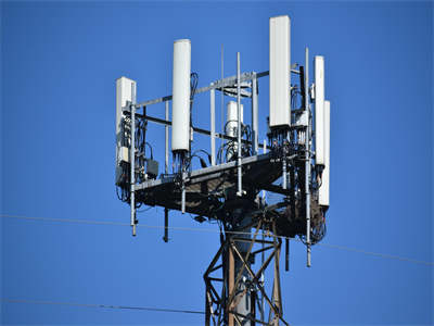
High-end communication equipment 1. 5G base station RF module 2. High-Speed Backplane Connectors |
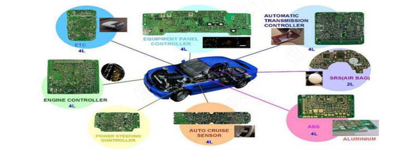
Automotive Electronics 1. Engine Control Unit 2. ADAS system circuit board |
|
  |
  |
  |
|
Aerospace 1. Satellite communication equipment 2. Flight Control System |
Medical electronics 1. Implantable devices 2. High-precision diagnostic equipment |
Industrial Control 1. Control panels for harsh environments 2. High reliability sensor |
The ENEPIG process faces several key challenges in practical applications:
Difficulty of process control: The thickness and uniformity of each coating layer need to be precisely controlled, and the phosphorus content deviation of the nickel layer needs to be controlled within ±1%
Operating cost pressure: The use of precious metal palladium leads to higher material costs, and the maintenance cost of the potion accounts for about 15-20% of the production cost
Talent demand: Professional technicians are needed to adjust process parameters, and the training cycle usually takes 3-6 months
Plating optimization: Developing 0.02μm ultra-thin gold layer technology, which can reduce gold usage by more than 30%
Cost control: Research and develop palladium alloy alternatives, and some companies have achieved a breakthrough of reducing palladium usage by 40%
Smart production: Introducing AI process control system to shorten parameter adjustment response time from hours to minutes
ENEPIG technology represents the latest development direction of PCB surface treatment and is particularly suitable for high-reliability and long-life electronic products. With the development of emerging technologies such as 5G, Internet of Things, and autonomous driving, the requirements for PCB reliability will continue to increase, and the market share of ENEPIG process is expected to continue to grow. In the future, with process optimization and scale effect, the cost of ENEPIG will be further reduced, allowing it to replace traditional surface treatment processes in a wider range of applications.

We are committed to building a world-leading brand in circuit board assembly services, delivering the most reliable products and support to our customers. Our goal is to set a benchmark in the industry and actively contribute to the advancement of the electronics sector.


Our hours
24H

 IPv6 network supported