There are several types of printed circuit boards (PCBs), each of which is suitable for specific design requirements and uses. According to the complexity of the circuit structure and different application requirements, PCBs can be divided into three key types: single-sided, double-sided and multilayer. In this article, we will introduce the characteristics of the three PCB types and the applicable scenarios in detail.
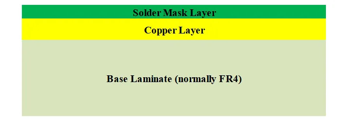
The simplest and least expensive type of PCB.
It has conductive wiring on one side only and substrate material on the other. These plates consist of a single conductive layer, usually composed of copper.Due to the simple structure, the single-panel production cost is low and the cycle time is short, which is very suitable for electronic products with simple circuits and a small number of components.
Specificities
- Single sided layout:Conductive lines are distributed only on one side of the PCB, and this simple and direct layout greatly reduces the difficulty of line layout.
- Cost-effective:Due to the simple structure, the production process is relatively easy, so that the single panel in the production cost occupies a clear advantage. Both the procurement cost of raw materials and the processing cost in the production process are at a lower level.
- Short cycle production:The simplicity of the production process means that single panels have a shorter lead time, allowing for a quick response to market demand and meeting the flexibility required for small batch production.
Application scenario
- Low-end consumer electronics:In fields such as toys and remote controls, electronic products have relatively simple functions and do not require high circuit complexity. With its advantages of low cost and rapid production, single panel becomes the ideal choice for these products, which can effectively reduce production costs and improve the market competitiveness of products.
- Space and weight sensitive scenarios:In some occasions where space and weight requirements are not high, the miniaturised, lightweight design of single sided pcb can meet basic usage requirements while achieving cost optimisation.
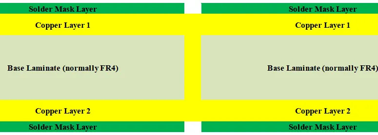
Dual or double-sided PCBs can be wired and soldered on both sides with an insulating layer in the middle, similar to single-sided PCBs, which also consist of a substrate. The difference, however, is that double-sided boards have conductive layers on both sides of the substrate, and these layers are interconnected through vias to create more complex circuit designs. Double-sided PCBs are one of the most widely used types of PCBs for electronic applications.
Specificities
- Double sided wiring:The conductive lines on both sides provide a wider space for circuit design, making the line layout more flexible and effectively improving the integration of the circuit.
- High circuit density:Compared to single sided PCBs, double sided PCBs enable higher circuit density, reduce signal interference and transmission delay problems caused by long lines, and improve circuit stability and reliability.
- Moderate cost and scale fit:Although double sided PCB is more complex than single sided PCB in terms of production process and relatively high cost, it is still at a moderate level. This increase in cost is matched by an increase in performance, and at the same time, it is suitable for medium-sized production and can meet the needs of most companies in the balance between production scale and cost control.
Application scenario
- Consumer electronics:Consumer electronics products such as mobile phones and tablet PCs have increasing circuit complexity and performance requirements. Dual-sided boards are able to meet the demands of complex circuit design while controlling costs and achieving intelligent and multi-functional products.
- Industrial control and communication equipment:Industrial control equipment and communication equipment need to have high reliability and stability. The high circuit density and good performance of double sided PCBs are one of the first choices in these fields as they can effectively reduce signal interference and ensure the normal operation of the equipment.
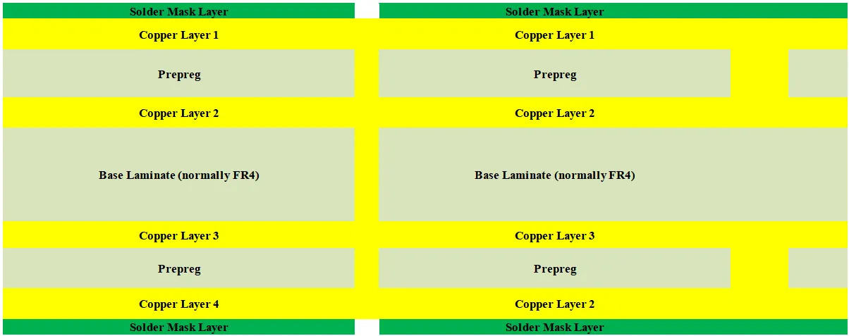
Multilayer PCBs are complex structures consisting of three or more layers of conductive traces and substrate materials alternately stacked on top of each other. Through clever over-hole design(through, blind and buried holes),realisation of electrical connections between different layers,These boards are often used in complex devices that require a large number of connections as a way to implement highly complex circuit designs and improve functionality.
Specificities
- Ultra-high circuit density:Multilayer structures provide nearly unlimited wiring space for circuit design, enabling extremely high circuit densities. Complex product functions, such as high-speed data processing and multi-channel signal transmission, can be perfectly realised on multilayer PCBs.
- Excellent electrical performance:The multilayer structure of the multilayer board and the rational use of insulating materials effectively reduce electromagnetic interference and signal crosstalk problems. The superior electrical performance makes the high-level board perform well in high-frequency and high-speed circuits, and can meet the strict requirements for signal integrity of high-end electronic products.
- High cost and mass adaptation:The production process of multilayer PCB is complex, requiring sophisticated equipment and a strict production environment, so the production cost is high. However, it is suitable for large-scale, high-performance products, and can realise mass production under the premise of guaranteeing product quality, improving production efficiency and product consistency.
Application scenario
- High-end consumer electronics:Products such as computers and servers demand the highest performance and stability from their circuits. Multilayer PCBs provide strong support for these products with their excellent performance, meeting the needs of complex computing and high-speed data transmission.
- Large and complex systems:Large and complex systems such as communication equipment and satellite navigation systems involve a great deal of signal processing and data transmission. The high circuit density and superior electrical performance of multilayer boards ensure reliable system operation and are indispensable core components in these fields.
- Specialised equipment areas:Medical equipment, aerospace equipment and other specialised equipment have demanding requirements for circuit reliability and stability. The high performance and reliability of multilayer boards provide a solid guarantee for the safe operation of these devices.
How to choose?
Choosing the right type of PCB requires a comprehensive consideration of the complexity of the circuit design, the cost budget, the production scale and the final application scenario.
In short, if the circuit is simple and cost-sensitive, a single sided PCB is ideal; if the circuit is slightly more complex and requires a certain circuit density, a double sided PCB is more appropriate; and for high-end electronics and large complex systems, a multilayer PCB is the way to go.
Service providers who choose to know and understand the characteristics of single sided PCBs, double sided PCBs and multilayer PCBs and application scenarios,it will help you to make more reasonable choices in electronic product design, so as to create high-quality products with excellent performance and reasonable cost.


 IPv6 network supported