Leave A Message
Fill out the form with your requirements and quantities(PCB/ Component Sourcing/ PCBA), and upload your Gerber file & BOM list. We'll provide you with a free quote as soon as possible!
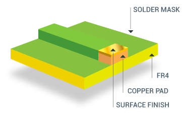
In the PCB (printed circuit board) manufacturing process,the surface treatment process directly affects its reliability, welding performance and service life. Different application scenarios have different requirements for surface treatment, so it is crucial to choose the right process. This article will introduce common PCB surface treatment methods, analyze their advantages and disadvantages and applicable scenarios, and help you make the best choice according to your needs.
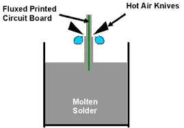

Features:Apply molten solder (tin-lead or lead-free) to the PCB surface and level it with hot air so that the solder evenly covers the copper surface.
Pros and Cons:
· Advantages: low cost, suitable for mass production, good welding performance.
· Disadvantages: poor surface flatness, not suitable for high-density interconnect (HDI) or fine-pitch components (such as BGA, QFN); leaded versions do not meet environmental requirements (lead-free HASL is more environmentally friendly).
Applicable scenarios:Ordinary consumer electronics, industrial control boards and other products that are cost-sensitive and have low welding requirements.
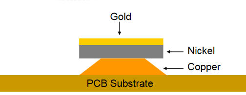

Features:A nickel layer is formed on the copper surface by chemical plating, followed by a thin layer of gold (usually 0.05-0.1 μm).
Pros and Cons:
· Advantages: Smooth surface, suitable for HDI and fine packaging; excellent welding performance, can be stored for a long time (about 12 months); lead-free and environmentally friendly.
· Disadvantages: Higher cost, may have "black disk" problem (nickel corrosion), affecting long-term reliability.
Applicable scenarios: Mobile phones, servers, automotive electronics and other products that have high requirements on reliability and welding performance.
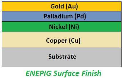

Features: Nickel, palladium and gold are plated on the copper surface in sequence (the gold layer is thinner, usually 0.03-0.05μm).
Pros and Cons:
· Advantages: More stable surface, avoids "black disk" problem, higher long-term reliability; excellent welding performance, compatible with gold wire and aluminum wire bonding; suitable for multiple welding and rework.
· Disadvantages: Highest cost and complicated process.
Applicable scenarios: High-end BGA, CSP packaging, automotive electronics, medical equipment, aerospace and other high reliability products.
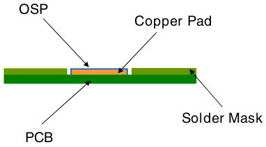

Features: Coat the copper surface with an organic protective film to prevent oxidation.
Pros and Cons:
· Advantages: low cost, environmentally friendly (no heavy metals), flat surface, suitable for HDI and fine pitch components.
· Disadvantages: short shelf life (3-6 months), storage environment needs to be strictly controlled; welding times are limited, and reworkability is poor.
Applicable scenarios: Consumer electronics, communication equipment and other cost-sensitive products with low soldering times.
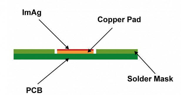

Features:Chemically plate a layer of silver (about 0.1-0.4μm).
Pros and Cons:
· Advantages: Good conductivity and welding performance, suitable for high-frequency applications (such as RF circuits); lower cost than ENIG and ENEPIG.
· Disadvantages: easy to oxidize, requires sealed packaging; poor reliability in long-term storage; there may be problems with silver ion migration.
Applicable scenarios:High frequency circuits, automotive electronics, and other applications that require electrical conductivity and welding performance.
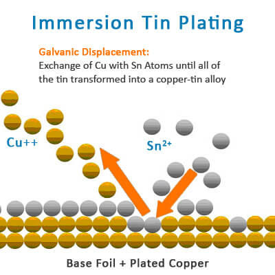

Features:Chemically plate a layer of tin (about 0.8-1.2μm).
Pros and Cons:
· Advantages: good welding performance, environmentally friendly and lead-free, suitable for HDI.
· Disadvantages: Easy to generate tin whiskers, affecting long-term reliability; high storage and welding conditions are required.
Applicable scenarios:Disadvantages: Easy to generate tin whiskers, affecting long-term reliability; high storage and welding conditions are required.
1. Choose by cost· Low cost: OSP, HASL (lead-free). · Medium cost: immersion silver, immersion tin. · High cost: ENIG, ENEPIG. |
2. Select according to welding requirements· Simple welding: OSP, HASL. · Precision soldering (BGA, QFN): ENIG, ENEPIG. |
3. Select by storage time· Short-term storage (<6 months): OSP, immersion silver. · Long-term storage (>12 months): ENIG, ENEPIG. |
4. Select by environmental requirements· Lead-free requirements: OSP, ENIG, immersion silver, immersion tin. |
5. Select by high frequency/conductivity requirements· High frequency circuit: immersion silver. |
6. Choose by reliability requirementsAutomotive, Medical, Aerospace: ENEPIG. |
The selection of PCB surface treatment process needs to comprehensively consider factors such as cost, welding performance, storage time, environmental protection and reliability.
· Consumer electronics: OSP or HASL is more cost-effective.
· High-end products (automotive, medical, aerospace): ENIG or ENEPIG are more reliable.

We are committed to building a world-leading brand in circuit board assembly services, delivering the most reliable products and support to our customers. Our goal is to set a benchmark in the industry and actively contribute to the advancement of the electronics sector.


Our hours
24H

 IPv6 network supported