Leave A Message
Fill out the form with your requirements and quantities(PCB/ Component Sourcing/ PCBA), and upload your Gerber file & BOM list. We'll provide you with a free quote as soon as possible!
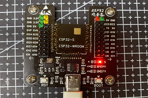
PCBA burning is the process of writing firmware into the chip to ensure that the hardware can work properly. The complete burning process usually includes the following key steps:
· Confirm the burned file: Check the firmware version and checksum to ensure that the file is correct.
· Check the device connection: Make sure the connection between the programmer (such as ST-Link, J-Link) and the PCBA is stable, and the interface (JTAG/SWD/UART) is not loose.
· Power supply check: Confirm that the power supply of the target board is stable (such as 3.3V/5V) to avoid programming failure caused by unstable voltage.
· Select chip model: Select the correct MCU model in the burning software (such as STM32CubeProgrammer).
· Configure the communication method: set the correct interface (JTAG/SWD/UART) and baud rate (such as 115200bps).
· Set protection options (optional): such as Read Protection and Write Protection.
· Erase chip: Clear the original data (erase the whole chip or erase the sector).
· Write firmware (Program): Write the firmware file (.bin/.hex) to the chip storage area.
· Verify: Read the chip content to ensure it is consistent with the programmed file.
· Simple test: Power on and check basic functions such as LED and serial port output.
· Full Test (optional): Run a full functional test to ensure that all modules are working properly.
· Save logs: record the burning time, operator, firmware version and other information for easy traceability.
· Mark PCBA: Use labels or ink to mark the burned boards to avoid repeated burning or confusion.
1. Programming Failed |
2. Verification Failed |
3. Device Not Recognized |
4. Abnormal function after burning |
5. Slow burning speed |
|
| Possible causes: |
· Connection problems: poor contact of the writer, damaged cables, oxidized interfaces. · Unstable power supply: Voltage fluctuations and excessive ripples lead to abnormal communication. · Chip protection: Flash write protection (Readout Protection) is not released. |
· The programming process is interrupted (such as power failure, communication interference). · The chip Flash is damaged (such as ESD breakdown). · The burning file is damaged (CRC check mismatch). |
· The writer driver is not installed (for example, ST-Link requires the driver to be installed). · The target chip model is incorrectly selected. · Communication interface configuration error (such as incorrect JTAG/SWD mode selection). |
· Wrong firmware version (e.g., an incompatible version was burned). · Clock configuration error (such as external crystal not enabled). · The chip configuration bits are set incorrectly. |
· The communication rate is too low (for example, the UART baud rate is set too low). · The performance limitation of the programmer (such as a slow programmer). · The firmware file is too large (for example, it exceeds the chip Flash capacity). |
| Solution: |
· Check the connection of the writer and re-plug the interface. · Use an oscilloscope to measure the power supply stability and add filter capacitors if necessary. · Remove the protection in the burning software (such as Option Bytes setting of STM32). |
· Re-burn to ensure the process is not interrupted. · Replace the chip or check the PCB for short circuit. · Regenerate the firmware file and check the MD5/CRC checksum.
|
· Install the correct burner driver. · Confirm the chip model and check the burning software support list. · Try switching JTAG/SWD mode, or reducing the communication rate (e.g. from 1MHz to 100kHz). |
· Verify that the firmware version matches the hardware. · Check the clock tree configuration (such as whether HSE/LSE is enabled). · Recheck the Option Bytes or Fuse Bits settings of the chip. |
· Increase the communication rate (such as UART from 9600bps to 115200bps). · Use a high-speed programmer (such as one that supports multi-channel parallel programming). · Optimize firmware size and delete unnecessary code segments. |
PCBA burning is a key step in the mass production of electronic products to ensure that the firmware is correctly written into the chip. The complete burning process includes preparation, parameter setting, burning execution, functional verification and recording. Common problems such as burning failure, verification error, device not recognized, etc. can usually be solved by checking the connection, power supply, chip protection, etc.
Best Practices Recommendations:
1. Standardized process: Establish a clear burning SOP (standard operating procedure).
2. Log management: Record detailed information of each burning to facilitate problem tracing.
3. Maintain equipment regularly: Check the reliability of the programmer, cables, and interfaces.
By standardizing operations and quickly troubleshooting problems, the success rate of burning can be improved and the stable production of PCBA can be ensured.

We are committed to building a world-leading brand in circuit board assembly services, delivering the most reliable products and support to our customers. Our goal is to set a benchmark in the industry and actively contribute to the advancement of the electronics sector.


Our hours
24H

 IPv6 network supported