Leave A Message
Fill out the form with your requirements and quantities(PCB/ Component Sourcing/ PCBA), and upload your Gerber file & BOM list. We'll provide you with a free quote as soon as possible!
AOI (Automatic Optical Inspection) is a core quality inspection tool for SMT (Surface Mount Technology) production lines. Using high-resolution cameras, multi-angle LED lighting, and intelligent image analysis algorithms, it performs real-time visual inspection of printed circuit board assemblies (PCBAs). Its core goal is to identify component placement defects (such as missing components, offset components, and incorrect polarity) and soldering quality issues (such as cold solder joints, bridging, and abnormal solder content), replacing traditional manual visual inspection to achieve efficient and accurate quality control.
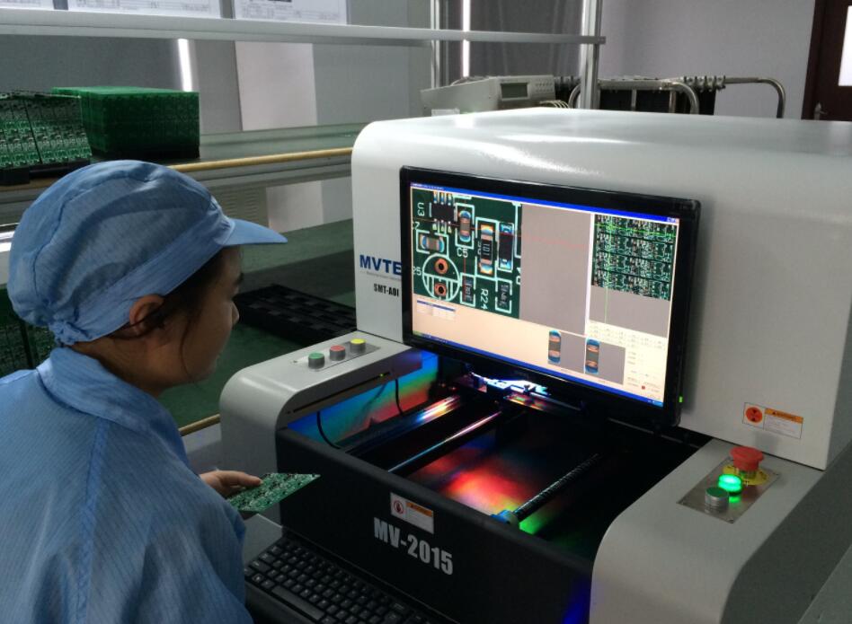
Figure 1: Practical application of AOI equipment in SMT production lines
Why do we need AOI?
As electronic products become thinner, lighter, and smaller (for example, the spacing between components on mobile phone motherboards has been reduced to 0.2mm), manual visual inspection faces three major pain points: low efficiency, poor accuracy, and weak consistency. AOI, by replacing humans, can increase inspection speed by more than 10 times and reduce the false positive rate to less than 1%, making it a key tool for ensuring soldering quality and improving production line yields.
The core of AOI is to complete the inspection through three steps: "image acquisition → image processing → defect determination":
· High-resolution camera: Uses 5-20 megapixel industrial cameras to capture micron-level details on the PCBA surface.
· Multi-angle lighting system: Combining red, blue, white, and ring-shaped light sources eliminates reflective interference (such as copper foil areas) and highlights key features such as solder joints and component edges.
· Preprocessing: denoising, contrast enhancement, and improving image clarity.
· Feature extraction: Identify component outlines and solder joint shapes through edge detection, template matching, and other technologies.
· AI Deep Learning (High-end Equipment): Trains models based on historical data to dynamically optimize defect judgment criteria (such as microcrack morphology in cold solder joints).
· The captured image is compared with the preset "standard template" (perfect placement/welding state). If the difference exceeds the threshold (such as the solder joint area is 20% smaller), it is marked as a defect.
· The results are transmitted to the MES system in real time, triggering an alarm or automatically rejecting defective products, and recording data for process optimization.
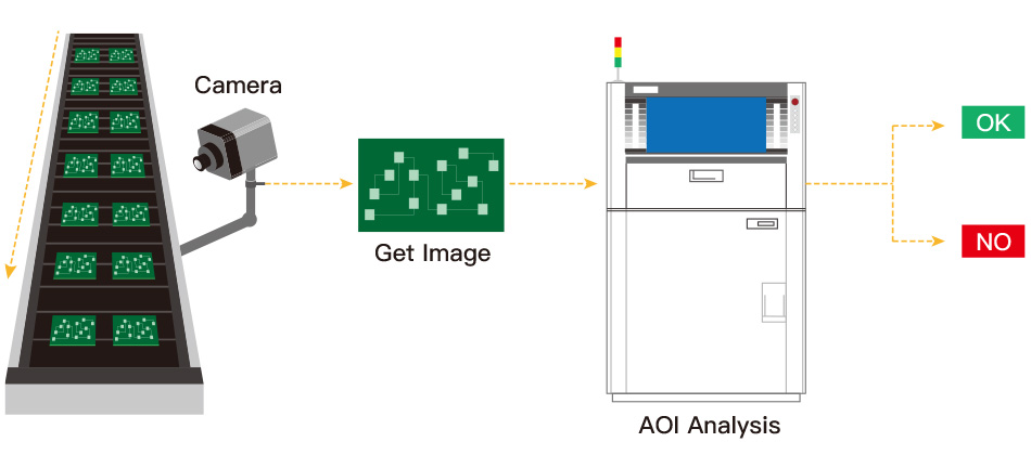

Figure 2: AOI inspection process diagram
· Component miniaturization: 0.2mm pitch QFP/SOP components are easily missed during manual visual inspection.
· Soldering becomes more complicated: Lead-free solder has a higher risk of oxidation, making defects such as cold solder joints and solder beads more hidden.
· Efficiency requirements: The production line has a fast cycle time (e.g., 60 PCBAs per minute), and manual labor cannot keep up with the speed.
|
Comparison Items |
AOI inspection |
Manual visual inspection |
|
Detection speed |
100-300 components/second |
20-30 components/minute |
|
Defect recognition accuracy |
0.1mm level (such as tiny solder bridges) |
Relying on experience, it is easy to miss small defects |
|
consistency |
Stable and not affected by fatigue |
Easy to fatigue, misjudgment rate 5%-10% |
|
Data traceability |
Automatically record test data |
Reliance on paper records makes tracing difficult |
· Reduce repair costs: Intercept defective products early to prevent them from entering the reflow or assembly process and becoming scrapped.
· Improved yield: In one case, the introduction of AOI increased the production line yield from 95% to 99.5%.

AOI covers a wide range of inspections from traditional components to special-shaped parts:
· Conventional components: rectangular chip components (0805/0603), cylindrical capacitors, tantalum capacitors, connectors.
· Precision components: QFP (0.4mm pitch), SOIC, BGA (requires X-ray inspection).
· Special components: coils, transistors, resistors, and special-shaped structural parts.
· Missing/Extra Components: Detects if components are missing or duplicated.
· Offset/Standing: Identifies components that are offset (>0.1mm) or standing upright ("tombstone" phenomenon).
· Wrong polarity: Check if the polarity of capacitors, diodes, etc. is correct.
· Flip/Wrong Parts: Determine if the component is reversed or the wrong model.
· Too little tin/too much tin: Insufficient or excessive amount of solder (affecting electrical connection or mechanical strength).
· Cold Solder Joint: The solder joint is not completely fused and there is a small gap.
· Bridging/short circuit: Excessive soldering between adjacent solder joints causes conduction.
· Solder Balling/Lifting: Solder balls flying off or solder joints lifting off the pad.
In SMT production, AOI, through high-speed, high-precision visual inspection, has become a key component in ensuring soldering quality and component assembly accuracy. With the integration of AI algorithms and 3D inspection technology, AOI will further enhance its ability to identify minute defects (such as BGA voids) in the future, helping electronics manufacturing move toward the goal of "zero defects."
Tip: When selecting AOI equipment, pay attention to three key indicators: inspection speed (matching the production line cycle), defect detection rate (>99%), and software usability (support for fast programming).

We are committed to building a world-leading brand in circuit board assembly services, delivering the most reliable products and support to our customers. Our goal is to set a benchmark in the industry and actively contribute to the advancement of the electronics sector.


Our hours
24H

 IPv6 network supported