Leave A Message
Fill out the form with your requirements and quantities(PCB/ Component Sourcing/ PCBA), and upload your Gerber file & BOM list. We'll provide you with a free quote as soon as possible!
As electronic devices progress toward miniaturization and higher performance, chip packaging technology for printed circuit boards (PCBs) continues to evolve. Ball Grid Array (BGA), a high-density, high-reliability packaging technology, has become a key technology in modern PCB design. This article will detail the basic principles, structural characteristics, advantages, and challenges of BGA technology.
BGA (Ball Grid Array) is a type of surface mount technology (SMT) in which the chip's pins are arranged on the bottom of the package in the form of solder balls, rather than traditional pins (such as the gull-wing pins of a QFP). These solder balls are directly soldered to the pads on the PCB, achieving an electrical connection between the chip and the circuit board.
|
Characteristic |
BGA |
Traditional QFP (Quad Flat Package) |
|
Pin arrangement |
Solder ball array (bottom) |
Pins (side) |
|
Pin density |
High (can accommodate hundreds of pins) |
Low (usually dozens of pins) |
|
Welding reliability |
Higher (good solder ball coplanarity) |
Lower (pins are easily deformed) |
|
Signal transmission |
Shorter paths, lower latency |
Longer paths, poorer signal integrity |
|
heat dissipation capacity |
Better (can dissipate heat through the bottom layer) |
Poor |
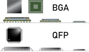
Figure 1: BGA vs. QFP package comparison
BGA package mainly consists of the following parts:
1. Chip (Die): core integrated circuit.
2. Substrate: Usually a multi-layer PCB material used to connect chips and solder balls.
3. Solder Balls: Small metal balls (usually tin-lead or lead-free alloy) on the bottom, used for soldering to the PCB.
4. Mold Compound: Protects the chip and internal interconnects.
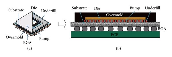
 Figure 2: Internal structure of a BGA package
BGA solder balls are usually arranged in a grid array. Common ones include:
· PBGA(Plastic BGA):Plastic packaging, low cost, suitable for consumer electronics.
· CBGA(Ceramic BGA):Ceramic package, high temperature resistant, suitable for aerospace.
· TBGA(Tape BGA):Tape packaging, suitable for ultra-thin devices.
BGAs can provide hundreds of pins in a small package area and are suitable for high-performance processors (such as CPUs and GPUs) and large-scale FPGAs.
· Shorter signal paths: Reduce inductance and capacitance, improving signal integrity.
· Low impedance: Suitable for high-speed data transmission (such as DDR, PCIe).
· The solder balls directly contact the PCB, and heat dissipation efficiency can be improved through thermal vias or metal heat dissipation layers.
· The solder balls have good coplanarity, are not easy to loosen after soldering, and have stronger vibration resistance.

· BGA solder balls are invisible and difficult to perform with traditional manual soldering, often requiring reflow soldering or X-ray inspection.
· Voiding problem: Air bubbles may form inside the solder balls, affecting reliability.
· Traditional AOI (Automated Optical Inspection) has difficulty inspecting BGA solder joints and requires the use of X-ray or CT scanning.
· Repair requires a BGA reballing station, which is relatively expensive.
· Requires detailed pad design (such as solder mask openings).
· Vias and power planes need to be optimized to reduce signal interference.
BGA packages are widely used in various electronic devices due to their high pin density and excellent electrical performance, including:
Smartphones and tablets: Core chips such as CPUs and GPUs use micro BGA packages (e.g., 0.4mm pitch) to achieve a thin and lightweight design.
Wearable devices: Small devices such as smart watches and TWS earphones use BGA to save space.
CPU, GPU: Intel and AMD processors use large BGA packages (such as FC-BGA) and are directly soldered to the motherboard.
Motherboard chipset: Chips such as storage controllers use PBGA to provide stable high-speed data transmission.
ECU (Engine Control Unit): Adopts high-temperature resistant CBGA or TBGA to adapt to the harsh environment of automobiles.
ADAS systems: Autonomous driving chips (such as those from Tesla and Nvidia) use high-density BGA packaging.
PLC (Programmable Logic Controller): Industrial-grade BGA chip ensures long-term stable operation.
FPGA chips: Xilinx and Intel FPGAs use extra-large BGAs (1000+ pins) for complex logic processing.
BGA technology is a core component of modern PCB design, offering high pin density, excellent electrical performance, and reliable packaging. However, it also presents challenges in soldering, inspection, and repair. With the development of finer pitches (such as 0.8mm and 0.5mm BGAs) and advanced inspection technologies (such as 3D X-ray), BGAs will continue to play a vital role in high-performance electronic devices.

We are committed to building a world-leading brand in circuit board assembly services, delivering the most reliable products and support to our customers. Our goal is to set a benchmark in the industry and actively contribute to the advancement of the electronics sector.


Our hours
24H

 IPv6 network supported