Leave A Message
Fill out the form with your requirements and quantities(PCB/ Component Sourcing/ PCBA), and upload your Gerber file & BOM list. We'll provide you with a free quote as soon as possible!
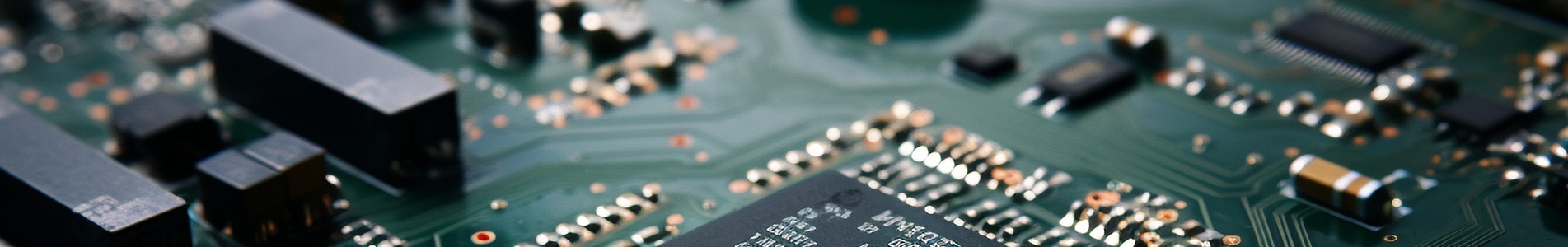
HDI PCB (High Density Interconnect PCB)It is an indispensable key component in modern electronic equipment, adopting micro-blind buried hole technology, its drilling diameter is less than 0.006 inches, more than 110 connections per square inch, with excellent signal transmission performance, which can effectively avoid interference and loss.
he manufacture of HDI PCBs involves a range of complex and advanced technologies. Among them,microblind buried hole technologyis the key.In the manufacturing process, it is necessary to use high-precision laser drilling equipment to create tiny through holes and blind holes (micro-blind holes connecting the surface layer to the inner layer, buried holes connecting the inner layer to the inner layer, and the outer layer is not visible), and then fill these holes with metal through plating and other processes to enhance the conductive properties of the hole wall and improve the electrical performance, so as to achieve the electrical connection between different layers. In addition, in order to meet the needs of high-density line layout, it is also necessary to use advanced graphic transfer technology, solder resist technology, etc., to ensure the accuracy and quality of the line.
From the point of view of the development of the manufacturing process, HDI PCBs have gone through a number of technology iterations. Currently common are first-order, second-order, third-order and even fourth-order process. The higher the order, the greater the complexity and density of the line, the greater the manufacturing difficulty also increases accordingly, but to meet the needs of higher-end electronic products. For example, some high-performance IC carrier boards need to use high-order HDI process to manufacture.
Mobile phones are one of the largest application markets for HDI PCBs, with more than 90% of mobile phone motherboards on the market using HDI technology. In addition, digital cameras, video cameras, MP3, MP4, notebook computers and other consumer electronics products are also widely used HDI PCB. with consumers on the performance of electronic products and portability requirements continue to improve, HDI PCB in this field of application prospects are very broad.
More and more electronic systems in modern automobiles, such as engine control systems, airbag systems, in-car entertainment systems, etc., rely on PCBs to achieve a variety of functions. HDI PCBs, with their high performance and reliability, can meet the stringent requirements of automotive electronic systems for signal transmission speed, stability, and safety, and are becoming more and more common in the field of automotive electronics applications.
In communication equipment, such as base stations, routers, etc., a large number of high-speed signals and data need to be processed.HDI PCB can provide a high-speed, stable signal transmission channel to ensure the normal operation of communication equipment. At the same time, with the continuous development of 5G technology, the performance requirements of PCB will be further improved, and HDI PCB will play a more important role.
The manufacturing process for HDI PCBs is extremely complex and technically demanding. During the manufacturing process, key parameters such as aperture size, aperture wall smoothness, and interlayer alignment accuracy need to be precisely controlled. As technology continues to advance, multi-stage HDI processes (e.g., second-, third-, and fourth-stage) have been developed to increase the number of layers and density of circuit boards, which, however, has also made production difficult and costly.
HDI PCB as the core component of the electronics industry, its high integration and high performance continue to promote the upgrading of electronic equipment. As technology continues to innovate, the performance requirements for HDI PCBs will also continue to improve HDI PCBs will continue to lead the industry's progress, providing a solid foundation for the development of science and technology. At the same time, the concept of environmental protection and sustainable development will also prompt the PCB industry to continue to innovate and develop more environmentally friendly, energy-saving HDI PCB products.

We are committed to building a world-leading brand in circuit board assembly services, delivering the most reliable products and support to our customers. Our goal is to set a benchmark in the industry and actively contribute to the advancement of the electronics sector.


Our hours
24H

 IPv6 network supported