Leave A Message
Fill out the form with your requirements and quantities(PCB/ Component Sourcing/ PCBA), and upload your Gerber file & BOM list. We'll provide you with a free quote as soon as possible!
In the design and manufacture of printed circuit boards (PCBs), signals and power are routed between different circuit layers through vias, and via design is a crucial step. Different types of vias (through, buried, and blind) are used to provide electrical connections, mechanical support, and thermal management.
There are three types of general PCB vias: through holes, blind holes, and buried holes:
1. Through Hole
A through hole is a hole that extends through the entire PCB layer, from the top layer to the bottom layer. These holes are commonly used to secure component pins to the PCB and provide electrical connections between different layers.
The advantages are that it provides a strong mechanical connection that can withstand high mechanical stresses, and the manufacturing process is relatively mature and cost-effective. However, the disadvantages are also significant: it occupies a large amount of PCB space, limiting high-density wiring. It can also affect signal integrity, especially in high-speed signal transmission.
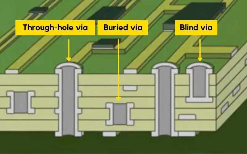
2. Blind Via
A blind via is a hole that extends from an outer layer of a PCB to an inner layer, but does not penetrate the entire PCB. It is used to connect electrical signals between an outer layer and one or more inner layers.
Blind vias significantly save PCB layout space, increase routing density, and improve signal integrity, making them suitable for high-speed signal transmission. However, the manufacturing process is complex and costly, and precise depth control is required, adding to the manufacturing complexity.
3. Buried Vias
Buried vias are holes located completely within a PCB, primarily used to connect electrical signals between two or more inner layers. They are not visible on the outer layers of the PCB.
Blind vias do not occupy outer layer space, increasing routing density. They enhance PCB design flexibility and are suitable for complex circuit designs. However, the manufacturing process is complex and costly. Precise manufacturing control is required, increasing production complexity.
Comparison and Selection
In PCB design, selecting the appropriate via type requires a comprehensive consideration of factors such as electrical performance, mechanical properties, manufacturing cost, and design complexity.
Through vias are suitable for applications requiring robust mechanical connections and offer lower costs, but are not suitable for high-density routing. Blind and buried vias are suitable for high-density, high-performance PCB designs, improving routing density and signal integrity, but at the expense of higher manufacturing costs.
Through, blind, and buried vias are essential elements in PCB design. Their respective characteristics and application scenarios determine their choice in different designs. As electronic products evolve towards miniaturization and higher performance, the use of blind and buried vias will become increasingly widespread.

We are committed to building a world-leading brand in circuit board assembly services, delivering the most reliable products and support to our customers. Our goal is to set a benchmark in the industry and actively contribute to the advancement of the electronics sector.


Our hours
24H

 IPv6 network supported