Leave A Message
Fill out the form with your requirements and quantities(PCB/ Component Sourcing/ PCBA), and upload your Gerber file & BOM list. We'll provide you with a free quote as soon as possible!
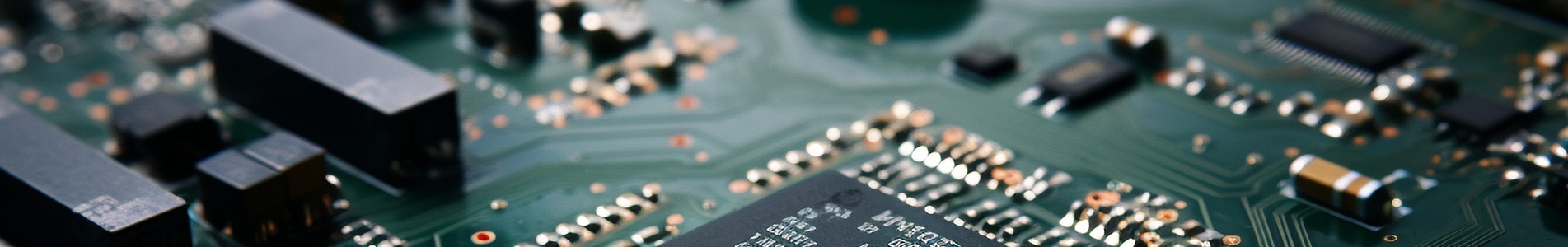
In the field of modern electronics, printed circuit boards (PCBs) connect the various electronic components in electronic devices and undertake the important tasks of signal transmission and circuit function realisation. Lithography is a critical and fundamental process in the PCB manufacturing process.
Lithography is essentially a projection exposure process. Photoresist is the key material in this technology, used to cover the copper layer part of the printed circuit board alignment pattern, it has a sensitivity to specific wavelengths of light, divided into two types of positive and negative. Positive photoresists undergo a chemical change in the part exposed to light, which is removed in the subsequent development process, while negative photoresists, on the contrary, become stabilised and retain the light-exposed part.
In practice, the PCB substrate is first coated with a uniform layer of photoresist, which is the basis for the entire lithography process. Subsequently, the pre-designed circuit pattern is projected onto the photoresisted PCB substrate by means of a photolithography mask (photomask). The mask plate has a transparent and an opaque part, and light can pass through the transparent part and be blocked by the opaque part. When the light is shone, an exposure area corresponding to the pattern of the mask plate is formed on the photoresist.


Coating photoresist can be done by spin-coating or spraying to evenly cover the PCB substrate. The thickness and uniformity of spin-coating can be precisely controlled by adjusting parameters such as rotational speed, which plays a crucial role in the manufacture of high-precision PCBs.
Exposure operations using photolithography require the precise selection of appropriate wavelengths of light, such as ultraviolet light, for exposure according to the different requirements of the circuit design. The exposure accuracy can reach the micron or even nanometre level, which directly determines the fineness of the circuit lines on the PCB.。
After exposure, the PCB substrate is immersed in the developer solution for development. If a positive photoresist is used, the exposed portion will be dissolved by the developer; whereas after the negative photoresist is developed, the unexposed portion will be removed, resulting in the desired pattern.
After developing, the PCB substrate is etched using an etching solution. Etching solution will accurately remove the substrate material that is not protected by photoresist, thus forming a precise circuit pattern, the accuracy and uniformity of Etching will directly affect the quality of the PCB.
At the end of the Etching operation, the photoresist is removed from the PCB substrate using a specific solvent, and the complete circuit pattern is now clearly visible on the PCB substrate.
III. Advantages of Lithography
Lithography has the advantage of high resolution, can create tiny circuit features, such as tiny Pad, fine line alignment. Thanks to these tiny circuit features, modern electronic products are able to develop in the direction of miniaturisation and high performance. For example, in smart phones and tablet computers and other devices with high space and performance requirements, PCBs made by lithography can integrate a large number of electronic components in a limited space to achieve complex and diverse functions.

We are committed to building a world-leading brand in circuit board assembly services, delivering the most reliable products and support to our customers. Our goal is to set a benchmark in the industry and actively contribute to the advancement of the electronics sector.


Our hours
24H

 IPv6 network supported