Leave A Message
Fill out the form with your requirements and quantities(PCB/ Component Sourcing/ PCBA), and upload your Gerber file & BOM list. We'll provide you with a free quote as soon as possible!

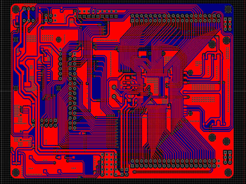
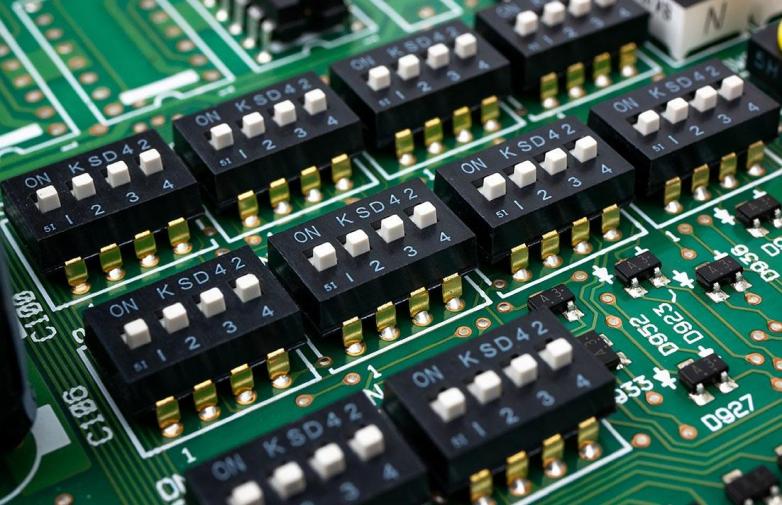
Copper layer is the core part of the PCB to assume the function of conductive. It is like the city's "highway" for the current to provide a smooth passage, so that the various electronic components can be achieved between the signal transmission and energy transfer. In the design of the PCB, engineers through etching and other processes to remove the unwanted copper foil part, leaving a specific circuit pattern, thus forming a variety of conductive paths and connections. These complex circuit patterns ensure that the electronic components work together accurately to fulfil the various functions of the electronic device.
The thickness of copper foil is usually measured in ounces (oz), with 1oz (about 35 microns) and 2oz (about 70 microns) being common. Thicker copper foils are capable of carrying higher currents and are important in application scenarios where high power signals need to be transmitted or high currents need to be handled, while thinner copper foils are more suitable for high frequency circuits, reducing losses in signal transmission and improving the efficiency of the circuit.
In addition, according to different application requirements, copper foil can also be divided into soft state and hard state. Flexible PCBs use soft state copper foil, which can adapt to the needs of bending and folding.
II. Solder mask layer : the board's security guards

The solder mask layer covers the surface of the PCB, like a layer of solid & ldquo; armour & rdquo;, to provide a full range of protection for the circuit board. Its main role is to prevent the welding process in the copper foil is oxidised, because the oxidation of the copper foil surface will form an insulating layer, affecting the welding quality and electrical connection performance. At the same time, the solder mask layer can also effectively avoid the occurrence of short-circuit phenomena, preventing the current from flowing in the inappropriate path, to ensure the stability and safety of the circuit.
In addition, it protects circuits from environmental moisture, dust and chemicals, extending the life of the board.
Currently, the common solder resist materials on the market include liquid photoimaging solder resist ink (LPI) and dry film solder resist.LPI has good resolution and adhesion, and can achieve fine pattern printing, suitable for high-density circuit design; dry film solder resist has better mechanical properties and chemical stability, more reliable protection, suitable for circuit boards of high quality requirements of the occasion.
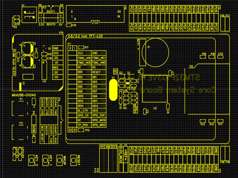
Although the legend layer does not directly affect the conductivity of the circuit like copper and solder mask layer, it plays an indispensable role in the identification and maintenance of circuit boards. It is printed with letters, numbers and symbols, labelled with component locations, models and other information to facilitate engineers to identify, assemble and repair circuit boards.
When designing the legend layer, the clarity and readability of the information needs to be taken into account. Silk-screen printing materials are mostly selected from epoxy resin or polyurethane inks, which have good adhesion and abrasion resistance, and can ensure that the text and symbols printed on the PCB surface are clear and long-lasting. At the same time, the colour of the legend layer is usually chosen to contrast with the background, such as white, for easy identification. In addition, reasonable layout and typography are also key to the design of the legend layer, to avoid overcrowding or intersection of information, and to ensure that the various markings are clear at a glance.
The copper layer, solder mask layer and legend layer each play a different role in the PCB, and there are clear differences between them.
Despite their different functions, in the PCB design and manufacturing process, they cooperate and work together to form a complete and efficient electronic circuit system.
The structure of PCB is a complex and sophisticated system, in which the copper layer, solder mask layer and legend layer are indispensable and important parts. They each play a unique role, synergise with each other, and provide a solid foundation for the stable operation of electronic equipment. In the future development of electronic technology, with the continuous upgrading and innovation of electronic products, the performance and requirements of PCB will be increasingly high. In-depth understanding and mastery of the function and characteristics of each layer in the PCB structure will help us to promote the continuous progress of electronic technology, in carrying out the PCB manufacturing industry continues to deepen.

We are committed to building a world-leading brand in circuit board assembly services, delivering the most reliable products and support to our customers. Our goal is to set a benchmark in the industry and actively contribute to the advancement of the electronics sector.


Our hours
24H


 IPv6 network supported