In PCB design, vias are key structures for interconnecting multi-layer circuits. Based on their penetration range and manufacturing process, vias are mainly divided into three types: through vias, blind vias, and buried vias. This article will systematically analyze their technical features and application scenarios.
I. Through Via
|
Definition:
A via that goes through all layers of a PCB, from the top layer to the bottom layer. This is the most traditional and widely used type of via, which goes through layers 1-2-3-4 in a four-layer board.
Manufacturing process:
Mechanical drilling is usually used, with a hole diameter of 0.2mm; high-density boards use laser drilling, with a hole diameter of up to 0.1mm. Electroplating is required to form a conductive path to support the installation of plug-in components and inter-layer signal transmission.
|
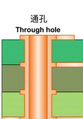 |
Features and Applications:
· Advantage:The process is mature and the cost is low, which is suitable for large current/mechanical fixing requirements (such as screw holes);
· Shortcoming:/strong>It occupies vertical space, affects wiring density, and high-speed signals may cause interference due to overly long routing;
· Typical Applications:General circuit board and power device mounting area.
Design points:
The aperture needs to meet electrical (current carrying capacity) and mechanical (pad size) requirements, and the solder mask treatment needs to prevent tin bead contamination.
|
II. Blind Via
|
Definition:
A non-penetrating hole that only connects the surface layer to the inner layer, usually from the top layer to the second layer or the bottom layer to the second to last layer. For example, a short via extending from the surface layer to the inner layer.
Manufacturing process:
· Laser blind via:The precision reaches ±0.025mm, which is suitable for HDI high-density interconnection boards;
· Mechanical blind hole:The cost is lower but the depth accuracy is limited (tolerance ±0.05mm).
Drilling copper plating must be completed before lamination, and depth control needs to consider the material expansion coefficient and plating uniformity.
|
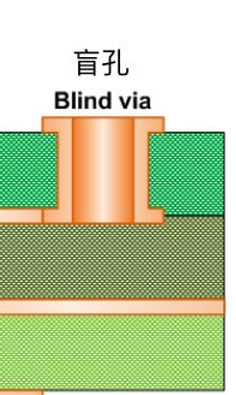 |
Features and Applications:
· Advantage:Save surface space, shorten signal paths (reduce impedance by about 30%), and improve high-frequency signal integrity;
· Shortcoming:The drilling accuracy requirement is high (depth ≤ 6 times of the hole diameter), and the defective rate affects the cost;
· Typical applications:Space-sensitive scenarios such as mobile phone motherboards, RF circuits, and ultra-thin devices.
Design Standards:
IPC-6012 Class 3 requires a blind hole depth-to-diameter ratio of ≤1:1 and a plating thickness of ≥0.8mil (20μm) to ensure reliable connection.
|
III. Buried Via
|
Definition:
The inner layer vias are completely hidden inside the multilayer board, connecting any two non-surface inner layers (such as L2-L5) and are not visible from the outside.
Manufacturing process:
Adopt layered lamination technology: first partial lamination + drilling copper plating, and finally integrate into a complete board. Multiple precise alignments are required (alignment deviation ≤15μm).
|
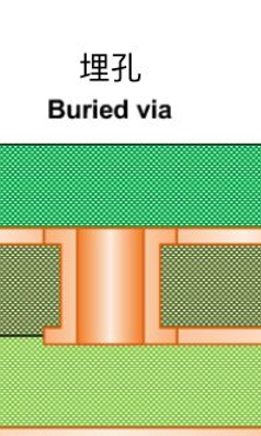 |
Features and Applications:
· Advantage:Maximize surface space release to achieve ultra-fine wiring (line width/spacing up to 3/3 μm) and eliminate through-hole shadow effect;
· Shortcoming:The process complexity is extremely high (cost increased by more than 40%), and rework is almost impossible;
· Typical applications:Large CPU substrates, optical modules, automotive radar PCBs and other high-density multi-layer boards.
Manufacturing Difficulties:
The inner hole diameter tolerance needs to be controlled within ±10%, and plasma cleaning is required after drilling to prevent residual glue from affecting the adhesion of the coating.
|
IV. Comparison Summary and Selection Guide
|
type
|
Penetration
|
Process complexity
|
cost
|
Applicable scenarios
|
|
Through Hole
|
Full-thickness penetration
|
Low
|
Low
|
Traditional circuit, power/ground signal
|
|
Blind Via
|
One-side penetration
|
Medium
|
Medium to high
|
HDI Board、High frequency and high speed design
|
|
Buried Via
|
Inner layer interconnection
|
High
|
Very high
|
Ultra-high density board, special fields
|
Key selection factors:
1. Density requirements: Blind vias are suitable for surface optimization, while buried vias are suitable for inner layer expansion.
2. Signal integrity: High-speed circuits give priority to buried/blind vias (signal delay reduced by 15%-25%)
3. Cost control: Through-hole ratio> 80% is an economical solution
V. Cutting-edge trends
· Ultra-micropore technology:Laser hole diameter exceeds 75 μm, achieving 10:1 aspect ratio in 5G base station PCB
· Electroplating process innovation:Vertical Continuous Plating (VCP) shortens the copper plating process by 30%
· Material improvements:Low dielectric constant laminates (Dk < 3.0) expand the upper limit of buried via applications
As electronic products evolve towards miniaturization and multifunctionality, the process maturity of blind and buried vias continues to improve. Designers need to comprehensively evaluate performance, cycle and cost,Develop optimal via design.


 IPv6 network supported