Leave A Message
Fill out the form with your requirements and quantities(PCB/ Component Sourcing/ PCBA), and upload your Gerber file & BOM list. We'll provide you with a free quote as soon as possible!
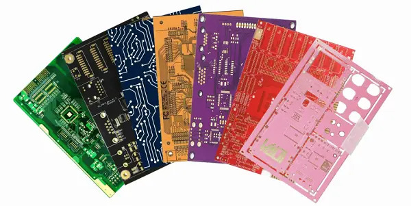
When you pick up a PCB, the first visual impact often comes from its bright colors: the classic green solder mask, the eye-catching white silk screen characters, or the dirt-resistant black coating on industrial equipment. These colors are not only a choice of design aesthetics, but also a functional decision that has been verified by long-term engineering. This article will deeply analyze the material science, process technology, cost structure of the solder mask and silk screen layer and their impact on product reliability, revealing the technical logic behind the color selection.
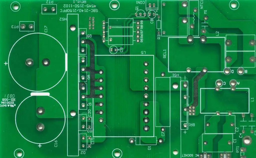
Solder mask is an insulating protective layer covering the conductive pattern of PCB. Its core function is to prevent solder bridging, resist environmental erosion, and provide precise positioning reference for subsequent assembly. Green solder mask has long dominated PCB manufacturing due to its mature process, cost advantages and excellent detection performance.
The procurement cost of mainstream green ink is 15-30% lower than that of special colors, and the supply chain is stable and reliable. In terms of optical inspection, green (L*≈55) and copper foil (L*≈20-30) form the best contrast, making the AOI system's false detection rate less than 0.1%, and the recognition of red solder repair marks on a green background is as high as 85%, which is significantly better than other color combinations. In addition, modern green solder mask ink has passed RoHS certification, and the glass transition temperature (Tg) after curing can reach above 150°C, which can not only meet environmental protection requirements, but also adapt to harsh application scenarios such as automotive electronics, achieving a perfect balance between performance and cost.
|
Color Type |
Typical application scenarios |
Process Challenges |
Cost increase |
|
White |
Display backlight panel (such as LED light panel) |
Requires high hiding power ink, easy to produce bubbles |
+20-40% |
|
Black |
Consumer electronics (such as mobile phone motherboards) |
Need to add carbon black pigment, the bending resistance is reduced |
+30-50% |
|
Blue |
Medical equipment (low fluorescence required) |
Special additives are needed to inhibit UV reflection |
+15-30% |
|
Red |
Repair Marking/Test Plate |
The curing temperature needs to be adjusted to avoid color difference |
+10-20% |
The silk-screen layer carries key information such as component identification, polarity marking, test point number, etc. Its design directly affects production yield and after-sales maintenance efficiency.
· Contrast calculation: White characters (L*≈95) form a high contrast of ΔE≈35 on green solder mask (meeting ANSI/IPC-7351 standard), which can be clearly identified even at a 30° tilted viewing angle.
· Ink characteristics: Use high hiding power epoxy resin-based ink (such as Sun Chemical 7100 series), adhesion ≥ Grade 1 (ASTM D3359), and solder resistance temperature can reach 260℃/10s.
· Line width limit: The minimum character width is recommended to be ≥0.8mm (corresponding to 7mil line width). Too thin may cause ink cracking (laboratory tests show that the cracking rate of 0.5mm line width in bending test is >15%).
· Height and spacing: The character height is usually 1.5-3mm, and the spacing is ≥1.2 times the character width to avoid accidental touch during assembly.
|
Application Requirements |
Recommended colors |
Technical considerations |
|
High temperature environment (such as engine compartment) |
Black |
Resistant to UV yellowing, but ink thickness needs to be increased(≥15μm) |
|
Yellow |
Reduce the risk of visual confusion between characters and pads |
|
|
Medical Devices |
Light Blue |
Meets IEC 60601-1-2 anti-glare requirements |
· Ink compatibility test:The interlayer adhesion of white silk screen ink and green solder mask layer must pass the 85℃/85%RH 1000h aging test (IPC-TM-650 standard), otherwise delamination may occur.
· Co-curing optimization:The risk of stress cracking can be reduced by using a staged curing process (e.g., first 150°C/3min solder mask curing, then 180°C/2min screen curing).
· White Laser Direct Structuring (LDS):It can replace traditional silk screen printing to realize dynamic identification of three-dimensional curved surface components (such as automotive HUD modules), but the cost is high (about $0.3/cm²).
· Smart solder mask ink: Add temperature-variable/light-variable pigments for anti-tampering marking (such as military equipment), and the color changes from green to red when the temperature changes (ΔT=50℃).
The color selection of PCB is not a simple aesthetic decision, but a deep combination of material science, manufacturing process, cost control and usage scenarios. The combination of green solder mask and white silk screen has become the industry standard due to its perfect balance between manufacturability, reliability and economy. With the miniaturization and multifunctional development of electronic products, more functional solder mask materials (such as self-healing ink) and intelligent silk screen technology may appear in the future, pushing PCB design into a new dimension.

We are committed to building a world-leading brand in circuit board assembly services, delivering the most reliable products and support to our customers. Our goal is to set a benchmark in the industry and actively contribute to the advancement of the electronics sector.


Our hours
24H

 IPv6 network supported